Setting Up the Integrated Logic Analyzer
Connecting a design to the ChipScope Integrated Logic Analyzer in order to debug at runtime

Introduction
In order to debug a FPGA design at runtime, steps must be taken in vivadeo to prepare the design and set up the ILA properly. This tutorial covers the process of selecting signals to debug as well as configuring the ILA to probe those signals. A follow up tutorial will cover using the ILA at runtime to view and debug signals.
Example Module
An example module containing a counter was written for this tutorial to illustrate the process of configuring the ILA. The verilog source and constraints used for the design are provided below.
module test_wrapper
(
	input clk, rst,
	input en,
	input [7:0] val,
	output A
);

    wire [7:0] count_out;

    //off if zero other wise turn on until counter reaches 'val'
    assign A = (count_out <= val)&(val!=0);

    counter_8_bit cnt_inst
    (
    	.clk(clk),
    	.rst(rst),
    	.en(en),
    	.val(count_out)
    );

endmodule


module counter_8_bit
(
	input clk, rst, en,
	output [7:0] val
);

	reg [7:0] count;

	assign val = count;


	always @(posedge clk)
	begin
		if(rst)
			count <= 0;
		else if(en)
			count <= count+1;
	end
endmodule
set_property -dict {PACKAGE_PIN H16 IOSTANDARD LVCMOS33} [get_ports clk]
create_clock -period 10.000 -name sys_clk_pin -waveform {0.000 4.000} -add [get_ports clk]

#btn 0 is enable to counter
set_property -dict {PACKAGE_PIN W14 IOSTANDARD LVCMOS33} [get_ports en]

#btn 3 is enable to rst
set_property -dict {PACKAGE_PIN M14 IOSTANDARD LVCMOS33} [get_ports rst]

#output LED
set_property -dict {PACKAGE_PIN N20 IOSTANDARD LVCMOS33} [get_ports A]

#value from switches
set_property -dict {PACKAGE_PIN R17 IOSTANDARD LVCMOS33} [get_ports {val[0]}]
set_property -dict {PACKAGE_PIN U20 IOSTANDARD LVCMOS33} [get_ports {val[1]}]
set_property -dict {PACKAGE_PIN R16 IOSTANDARD LVCMOS33} [get_ports {val[2]}]
set_property -dict {PACKAGE_PIN N16 IOSTANDARD LVCMOS33} [get_ports {val[3]}]
set_property -dict {PACKAGE_PIN R14 IOSTANDARD LVCMOS33} [get_ports {val[4]}]
set_property -dict {PACKAGE_PIN P14 IOSTANDARD LVCMOS33} [get_ports {val[5]}]
set_property -dict {PACKAGE_PIN L15 IOSTANDARD LVCMOS33} [get_ports {val[6]}]
set_property -dict {PACKAGE_PIN M15 IOSTANDARD LVCMOS33} [get_ports {val[7]}]
1. Mark Nets to Debug
In your the source file for the module you want to debug, mark any signals of interest. This is done using the following statement, prior to the signal declaration
(* mark_debug = "true", keep = "true" *)
This tells the synthesis tools that the wire is to be debugged and potentially connected to ILA cores in the system. It also tells the synthesis tool to make sure the signal is part of the circuit. Sometimes the synthesis processes can ‘cull’ extraneous resources used, this ensures you can see the signals you expect when debugging. The statement can be placed before signals in the module header as well as in the body of the module. In the example show below, the ‘test_wrapper’ module was modified to have a number of it’s signals marked for debug.
module test_wrapper
(
	input clk, rst,

	(* mark_debug = "true", keep = "true" *)
		input en,
	(* mark_debug = "true", keep = "true" *)
		input [7:0] val,
	(* mark_debug = "true", keep = "true" *)
		output A
);

    (* mark_debug = "true", keep = "true" *)
    	wire [7:0] count_out;

    //off if zero other wise turn on until counter reaches 'val'
    assign A = (count_out <= val)&(val!=0);

    counter_8_bit cnt_inst
    (
    	.clk(clk),
    	.rst(rst),
    	.en(en),
    	.val(count_out)
    );

endmodule
2. Run Synthesis
Now run the synthesis tool to produce a synthesized design.
If synthesis succeeds, you can then open your synthesized design using the ‘synthesis completed’ pop-up menu or in the flow navigator.
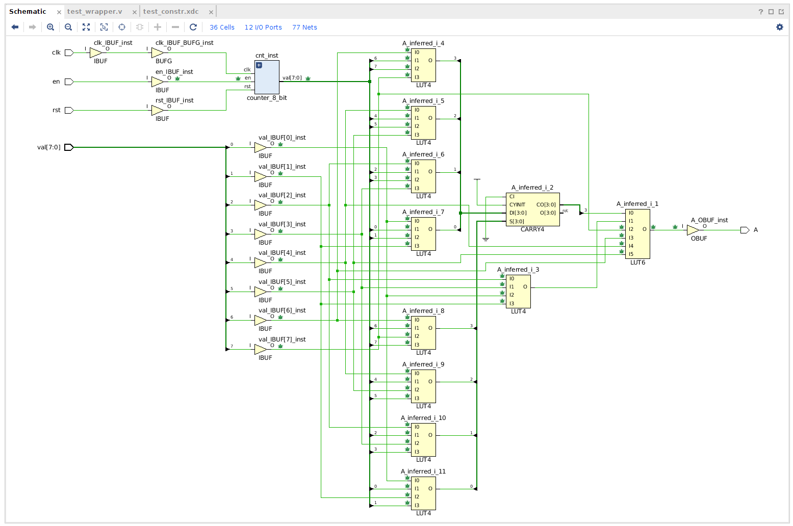
3. Open The Synthesized Design
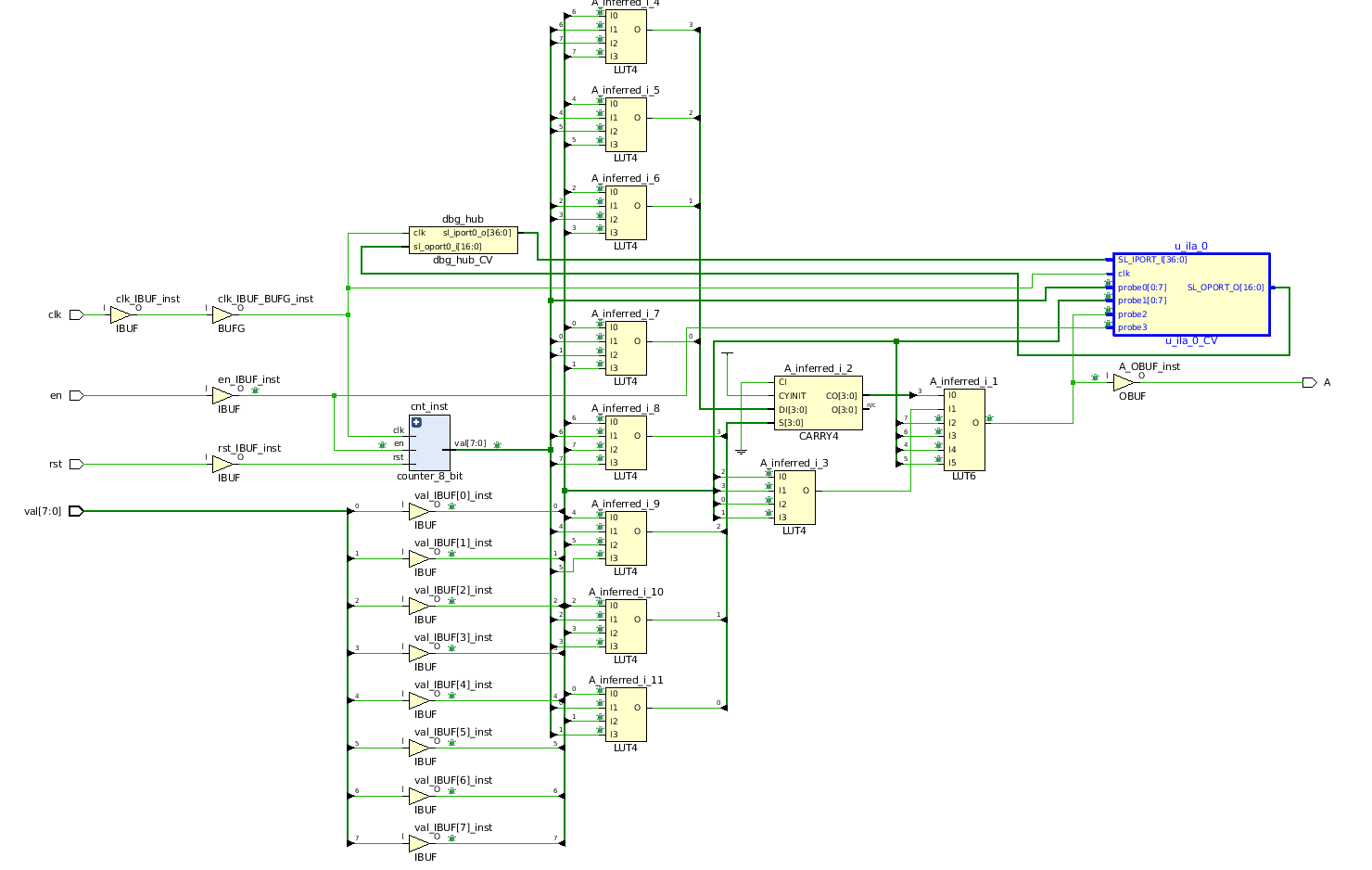
Now vivado will show the schematic of your synthesized design. This shows you how your actual circuit will be configured on the FPGA; The blocks shown correspond to the actual logic elements on the device. For instance, an LUT4 is a 4-input lookup table, and and an FDRE is D-flip-flop.
Your synthesized design is actually a list of ‘I/O ports’, ‘cells’, and ‘nets’ and the schematic view is a visualization of this list. I/O ports are the nodes which connect your design to external pins on the FPGA. Cells are the different kinds of devices found within the FPGA; These can be logic devices like LUT’s, output buffers, or various other devices. Nets are the interconnections between cells and/or ports.
If you have marked wires for debug in your source files, you will notice some of the nets in the schematic view are annotated with a little ‘bug’ icon. This indicates that the net has been selected for debugging.
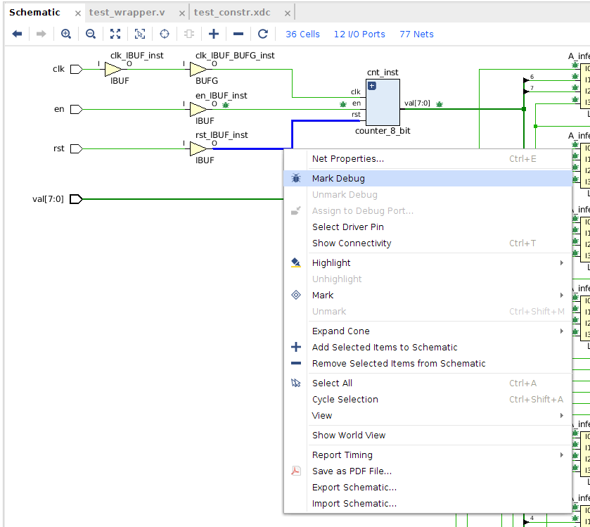
You can also mark and unmark nets for debug in the synthesized design schematic view. Right-clicking on the desired net will bring up the option to mark or unmark the selected net.
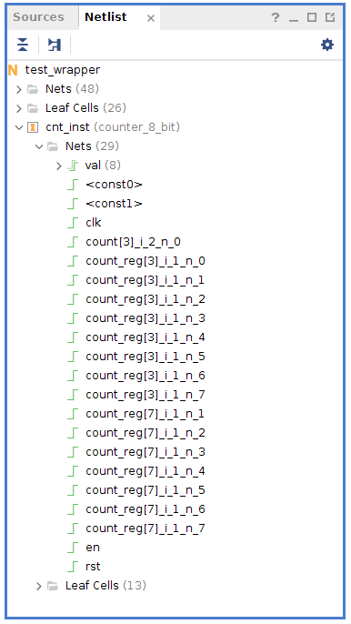
Another way to find nets in the synthesized design is through the netlist. Here you can also right click and mark nets for debugging.
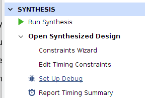
4. Set Up Debug
After you have selected the nets you want to see using the ILA, click on setup debug in the flow navigator (found under ‘open synthesized design’)
Follow the Dialogue to the ‘Nets to Debug’ view. Here you will see any nets you have previously selected. You can also add additional nets.
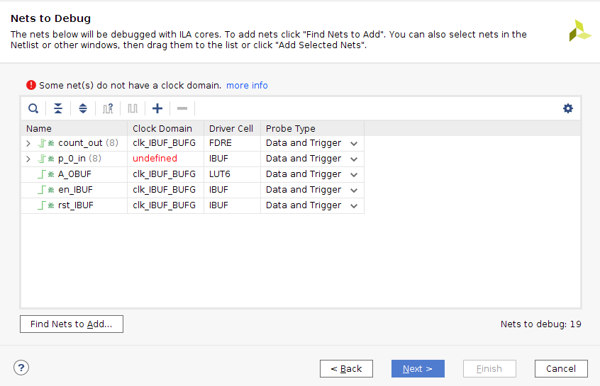
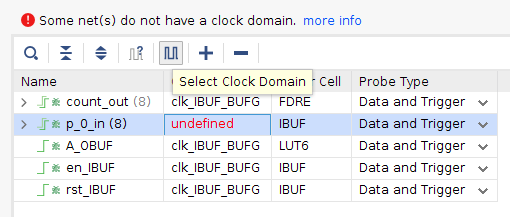
You will notice in our example there is a warning about some nets not having a clock domain. The tools will automatically attempt to associate clocks with synchronus signals that have been selected for debug. Since the input from the switches is clearly an asynchronus signal, the tools did not assign it a clock. It is interesting to note, that while the nets en and rst are also asynchronous, they were assigned a clock domain; as signals like en and rst are often synchronous signals the tools assumed that they were indeed and assigned them to a clock domain.
Associating clock domains
In the ILA, the clock domain selected for a signal will select which clock the ILA uses to sample that signal. That is, every clock cycle, the ILA core will capture the state of each signal. For synchronous signals it’s almost always a good idea to select the clock the signal is associated with. With asynchronous signals you need to be a bit more careful; If the signal is capable of changing faster than the sample clock, it cannot be accurately sampled. In general, the best practice is to sample with a clock at least 2.5 times the frequency of the fastest component of the signal.
Note: For designs with a single clock it is not an issue, but if signals are associated with multiple clock domains in this dialog, the tools will actually create one ILA core for each individual clock domain. As this can create a large burden on your device resources, you may want to use a single sample clock even if there are multiple clock domains. Similar to scoping to asynchronus signals, when doing this you should select a clock at least 2.5 times the frequency of the signals. Since the clock in the example design is 100MHz and all the asynchronous signals will be operated by hand, the sample rate as more than sufficient to accurately portray the signals.
To associate a clock, select the net(s) and click the ‘select clock domain’ icon. and in the following dialogue pick the appropriate clock.
Select Sample Depth
In the next dialogue you can set the sample depth. This is how many samples of each signal the ILA core will capture after being triggered. Since the sample rate of each ILA core is set by it’s sample clock, this means how long each capture will be; The clock period multiplied by the sample number of samples. In the example, the default depth of 1024 was kept, meaning each capture window will be 0.00001024s long.
Summary
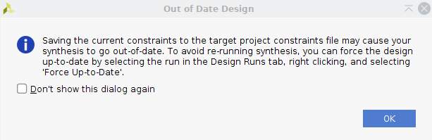
The final summary will tell you how many debug cores will be created and how many clocks found. Once you click ‘Finish’, your design will be modified. After completing the set up debug dialogue, save your synthesized design through the menu or using ctl+s when you are in the synthesized design view. Since the design has been set up for debug, the tool will notify you that your constraints file will be modified and then synthesis will go out of date. As this will modify the currently selected constraints, if you are using a ‘master’ .xdc file it is recommended you make a copy of this for each project, so modifying one project does not affect another.
Once you have saved the changes to your synthesized design, you can open up your constraints file and see that it has been modified. If you do not see changes, you might have to close and reopen it in the vivado editor. Shown below is the example module’s updated constraints
set_property -dict {PACKAGE_PIN H16 IOSTANDARD LVCMOS33} [get_ports clk]
create_clock -period 10.000 -name sys_clk_pin -waveform {0.000 4.000} -add [get_ports clk]

#btn 0 is enable to counter
set_property -dict {PACKAGE_PIN W14 IOSTANDARD LVCMOS33} [get_ports en]

#btn 3 is enable to rst
set_property -dict {PACKAGE_PIN M14 IOSTANDARD LVCMOS33} [get_ports rst]

#output LED
set_property -dict {PACKAGE_PIN N20 IOSTANDARD LVCMOS33} [get_ports A]

#value from switches
set_property -dict {PACKAGE_PIN R17 IOSTANDARD LVCMOS33} [get_ports {val[0]}]
set_property -dict {PACKAGE_PIN U20 IOSTANDARD LVCMOS33} [get_ports {val[1]}]
set_property -dict {PACKAGE_PIN R16 IOSTANDARD LVCMOS33} [get_ports {val[2]}]
set_property -dict {PACKAGE_PIN N16 IOSTANDARD LVCMOS33} [get_ports {val[3]}]
set_property -dict {PACKAGE_PIN R14 IOSTANDARD LVCMOS33} [get_ports {val[4]}]
set_property -dict {PACKAGE_PIN P14 IOSTANDARD LVCMOS33} [get_ports {val[5]}]
set_property -dict {PACKAGE_PIN L15 IOSTANDARD LVCMOS33} [get_ports {val[6]}]
set_property -dict {PACKAGE_PIN M15 IOSTANDARD LVCMOS33} [get_ports {val[7]}]

create_debug_core u_ila_0 ila
set_property ALL_PROBE_SAME_MU true [get_debug_cores u_ila_0]
set_property ALL_PROBE_SAME_MU_CNT 1 [get_debug_cores u_ila_0]
set_property C_ADV_TRIGGER false [get_debug_cores u_ila_0]
set_property C_DATA_DEPTH 1024 [get_debug_cores u_ila_0]
set_property C_EN_STRG_QUAL false [get_debug_cores u_ila_0]
set_property C_INPUT_PIPE_STAGES 0 [get_debug_cores u_ila_0]
set_property C_TRIGIN_EN false [get_debug_cores u_ila_0]
set_property C_TRIGOUT_EN false [get_debug_cores u_ila_0]
set_property port_width 1 [get_debug_ports u_ila_0/clk]
connect_debug_port u_ila_0/clk [get_nets [list clk_IBUF_BUFG]]
set_property PROBE_TYPE DATA_AND_TRIGGER [get_debug_ports u_ila_0/probe0]
set_property port_width 8 [get_debug_ports u_ila_0/probe0]
connect_debug_port u_ila_0/probe0 [get_nets [list {count_out[0]} {count_out[1]} {count_out[2]} {count_out[3]} {count_out[4]} {count_out[5]} {count_out[6]} {count_out[7]}]]
create_debug_port u_ila_0 probe
set_property PROBE_TYPE DATA_AND_TRIGGER [get_debug_ports u_ila_0/probe1]
set_property port_width 8 [get_debug_ports u_ila_0/probe1]
connect_debug_port u_ila_0/probe1 [get_nets [list {p_0_in[0]} {p_0_in[1]} {p_0_in[2]} {p_0_in[3]} {p_0_in[4]} {p_0_in[5]} {p_0_in[6]} {p_0_in[7]}]]
create_debug_port u_ila_0 probe
set_property PROBE_TYPE DATA_AND_TRIGGER [get_debug_ports u_ila_0/probe2]
set_property port_width 1 [get_debug_ports u_ila_0/probe2]
connect_debug_port u_ila_0/probe2 [get_nets [list A_OBUF]]
create_debug_port u_ila_0 probe
set_property PROBE_TYPE DATA_AND_TRIGGER [get_debug_ports u_ila_0/probe3]
set_property port_width 1 [get_debug_ports u_ila_0/probe3]
connect_debug_port u_ila_0/probe3 [get_nets [list en_IBUF]]
set_property C_CLK_INPUT_FREQ_HZ 300000000 [get_debug_cores dbg_hub]
set_property C_ENABLE_CLK_DIVIDER false [get_debug_cores dbg_hub]
set_property C_USER_SCAN_CHAIN 1 [get_debug_cores dbg_hub]
connect_debug_port dbg_hub/clk [get_nets clk_IBUF_BUFG]
This addition to your constraints file contains all of the information you provided to set up the debug. At any point to remove an ILA core you can comment out or remove the lines following ‘create_debug_core’.
To modify which signals you are probing, or if you have removed signals previously marked for debug, you need to run ‘set up debug’ from the synthesized design view again.
5. Synthesize the design with ILA Core
Now you can synthesize your module again, then open the synthesis view to see the ILA core has been added to your design. At this point you can implement your design and write a bitstream.
Conclusion
Once you have implemented the design, you can program the bitstream to your device. In vivado’s hardware manager you will be able to access the ILA Waveform Display. The use of the ILA Waveform is covered in a follow up tutorial titled “Using the Integrated Logic Analyzer”. This details steps to connect to the ILA, set up data capture triggers, and capturing data in the hardware manager.