XOR Gates

XOR Gates
The two-input exclusive-or (XOR) gate is a common circuit used in many digital applications. It is often used as a controllable toggle switch. The circuit, schematic symbol, and truth table are shown below.

The XOR gate outputs a 1 when either A is high or B is high, but not when both are high. In other words, the XOR gate outputs a 1 when an odd number of inputs are asserted. This circuit can be optimized to use just 12 transistors using CMOS technology.
The exclusive-NOR (XNOR) gate is very similar to the XOR gate, except with the addition of a NOT gate on the output. The XNOR gate outputs a 1 when an even number of inputs are asserted.
Think of a the XOR gate as a two-way light switch in your house: flipping any switch in the circuit toggles the light. Both the XOR and XNOR circuit can be written in Verilog as follows:
module xor_2 (
    input A, B,
    output Y
);
assign Y = A ^ B;
endmodule
module xnor_2 (
    input A, B,
    output Y
);
assign Y = ~(A ^ B);
endmodule
We can create a three-input XOR gate by cascading two-input XOR gates into another. A three-input XNOR gate can be made by cascading two-input XOR gates, and then adding a NOT gate to the output.

We can extend this idea to create an XOR or XNOR gate of any size. Shown below is an implementation of a 3-input XOR and XNOR gate in Verilog.
module xor_3 (
    input A, B, C,
    output Y
);
assign Y = A ^ B ^ C;
endmodule
module xnor_3 (
    input A, B, C,
    output Y
);
assign Y = ~(A ^ B ^ C);
endmodule
Pro Tip: We can simplify our code by using the XNOR reduction operator. In general, reduction operators are great choices when performing one operation multiple signals.
module xnor_3_reduced (
    input [2:0] X,
    output Y
);
assign Y = ~^X;
endmodule
Test Bench
To run this test bench, create a source file called xor_3.v and paste the xor_3 module from above. Do the same for the xnor_3 module. Create a new simulation file called xor_tb.v and paste the following code. Press the “Run Simulation” button and a similar waveform simulation will appear.
`timescale 1ns/1ps
module xor_tb;

// inputs are stored in registers since registers can hold values
reg A, B, C;

// outputs are assigned to wires
wire Y, Z;

// instantiate our xor_3 module, name this instance "CUT_1"
// we can change the name CUT_1 to just about anything we want
// "CUT" commonly stands for "Circuit Under Test"
xor_3 CUT_1 (
    .A(A),
    .B(B),
    .C(C),
    .Y(Y)
);

// connect the output of the xnor gate to wire "Z"
xnor_3 CUT_2 (
    .A(A),
    .B(B),
    .C(C),
    .Y(Z)
);

// run the simulation, testing all possible combinations of A, B, and C
integer k;
initial begin
    for(k = 0; k < 8; k=k+1) begin
        #10 {A,B,C} = k;
    end
    #10 $finish;
end

endmodule
A new tab should appear named “Untitled 1”. Click on it to view the simulation. Click the “Zoom Fit” button to see the entire simulation.
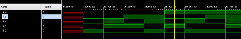
Verify that Y is a 1 when an odd number of inputs are asserted. Verify that Z is a 1 when an even number of inputs are asserted. Verify that Y and Z are always the “not” of each other.
Note: since there are three binary inputs to these circuits, there are 2^3 = 8 possible input combinations for A, B, and C. Each input combination tests one of the rows in the truth table for the three-input XOR and XNOR gates.
Important Ideas
- XOR and XNOR gates are common building blocks in digital design.
- XOR gates can be used as a controllable inverter by using one input as a control signal, and the other input as the data signal. Driving the control signal high results in the data signal fliping values.
- XOR gates can be used to check parity, i.e. if the number of ones in a signal is even or odd.