Simulating a Peripheral with AXI4-Lite interface
AXI Bus Simulation using Vivado Simulator

Using Vivado Simulator to Simulate a perippheral with AXI4-Lite interface
The Integrated Logic Analyzer is a very powerful tool for debugging hardware. However, Since it adds complexity to your design, implementation may take a long time. Becuase of this, it’s best practice to write a test bench to simulate IP cores before implementation. Simulation of an AXI4 IPcore requires emulating the signals on the AXI bus for write and read transactions. The Following Guide goes over the process of creating a AXI4 IP testbench and running simulation.
Step 1: Create a Test Bench for the myled AXI4-Lite Custom IP Core
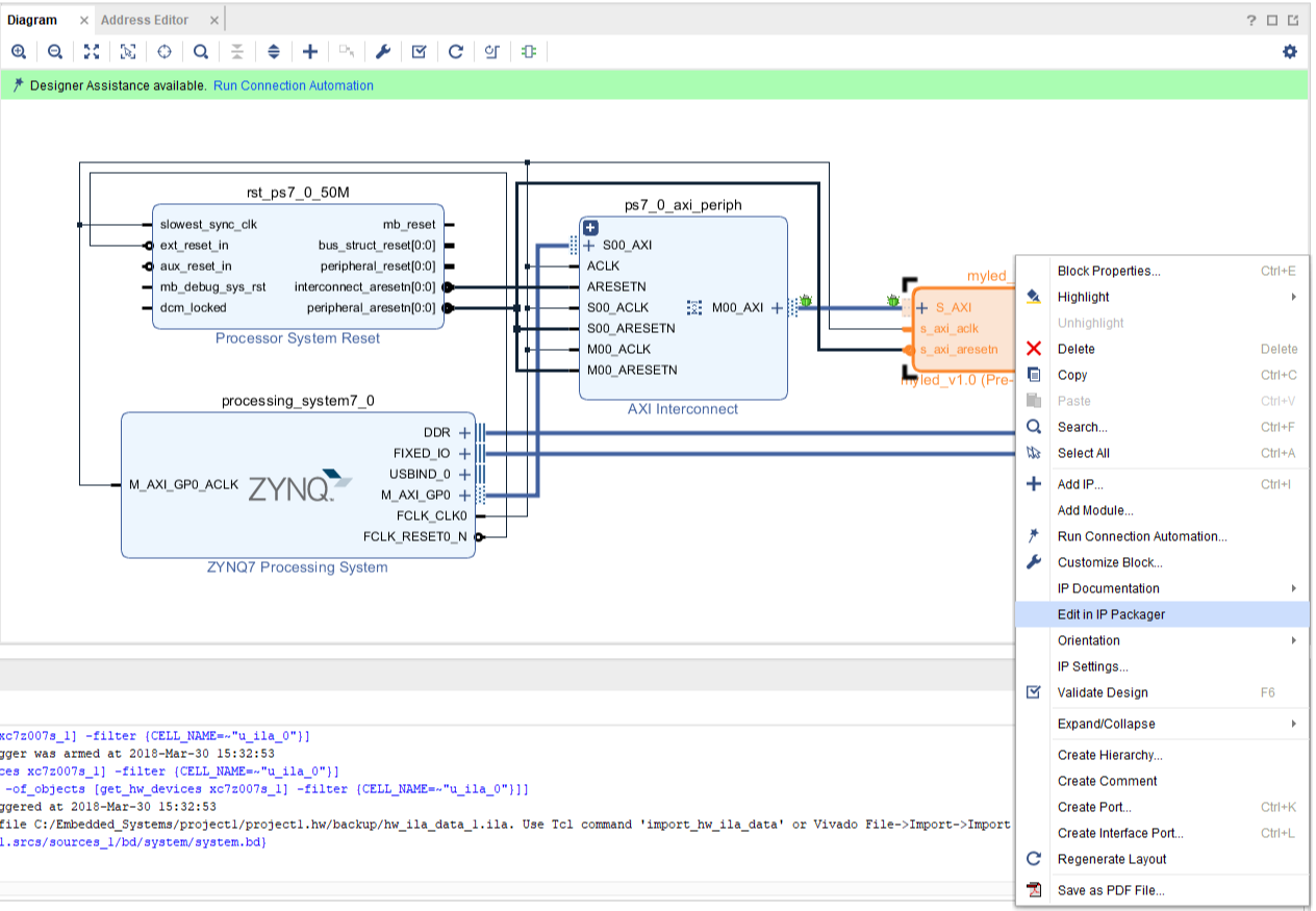
Open up the block design. Right click on myled IP and choose Edit in IP Packager as shown in figure 1. In your myled IP packager you can now create a a test bench and simulate your AXI4-Lite interfaces.
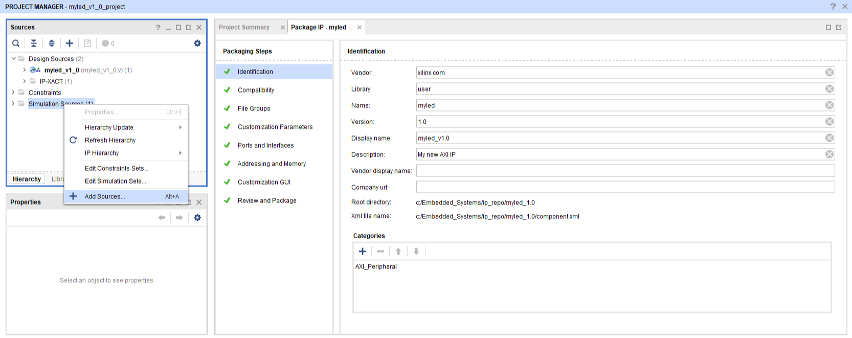
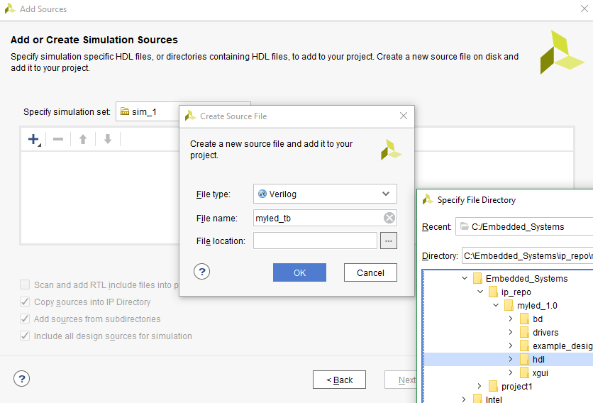
Right click on sim_1 under simulation sources and click Add Sources.
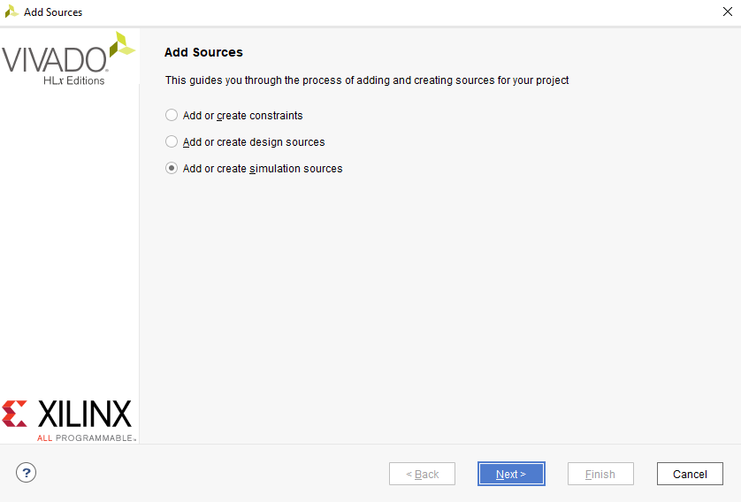
In the pop-up Add Sources dialog, select Add or create simulation sources and click Next.
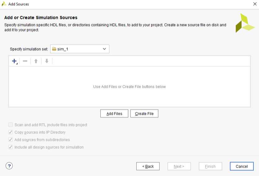
Click on Create File to create the test bench file.
In the pop up window, name the file myled_tb and select the hdl folder under myled_1.0 which can be found in your ip_repo directory. Click Finish to add myled_tb.v to simulation set sim_1 in the IP packager project.
Step 2: Form A Test Plan
Instead of going straight to writing a testbench, we should come up with a plan for how to simulate the IPcore. For our purpose we would like to simulate writing values, via the AXI bus, to the slave register which drives the LEDs. After the write is simulated properly, the 4 LED signals should reflect the 4 LSB’s of the 1st slave register.
Your plan, of course, should depend on your application. Make sure you have a suitable plan for each simulation you need.
Step 3: Implement the Test in Verilog
Instead of writing a testbench where the AXI4 signals are manipulated again and again in the main body of code, it would be best to write a single reusable sequence of code that takes an argument and drives signals accordingly. This can be accomplished using the task structure in Verilog. A task can be written and called in verilog to execute a sequence of operations. They can be parameterized to include inputs and outputs which can affect the operations and return results. Using tasks to handle simulation of AXI transactions will reduce code bulk in the main body of your testbench as well as improve readability.
For simulating the AXI bus, your tasks will need to drive the address, data, and response lines relevant to the transaction. The task will also need to respond to the handhsaking signals from the AXI4-lite slave (in this case the LED IPcore).
First step in writing a AXI4 testbench is to define all the signals used by the AXI4-lite interface. Since our Task will be controlling the Master signals, those should be set as reg type. The slave signals will be driven by our IPcore and should be wire's. Next, instantiate your IP core, making the appropriate port connections to the previously defined AXI4-lite signals.
`timescale 1ns /1ps

module myled_tb();

	//clock and reset_n signals
	reg aclk =1'b0;
	reg arstn = 1'b0;


	//Write Address channel (AW)
	reg [31:0] write_addr =32'd0;	//Master write address
	reg [2:0] write_prot = 3'd0;	//type of write(leave at 0)
	reg write_addr_valid = 1'b0;	//master indicating address is valid
	wire write_addr_ready;		//slave ready to receive address

	//Write Data Channel (W)
	reg [31:0] write_data = 32'd0;	//Master write data
	reg [3:0] write_strb = 4'd0;	//Master byte-wise write strobe
	reg write_data_valid = 1'b0;	//Master indicating write data is valid
	wire write_data_ready;		//slave ready to receive data

	//Write Response Channel (WR)
	reg write_resp_ready = 1'b0;	//Master ready to receive write response
	wire [1:0] write_resp;		//slave write response
	wire write_resp_valid;		//slave response valid

	//Read Address channel (AR)
	reg [31:0] read_addr = 32'd0;	//Master read address
	reg [2:0] read_prot =3'd0;	//type of read(leave at 0)
	reg read_addr_valid = 1'b0;	//Master indicating address is valid
	wire read_addr_ready;		//slave ready to receive address

	//Read Data Channel (R)
	reg read_data_ready = 1'b0;	//Master indicating ready to receive data
	wire [31:0] read_data;		//slave read data
	wire [1:0] read_resp;		//slave read response
	wire read_data_valid;		//slave indicating data in channel is valid

	//LED output of the IPcore
	wire [3:0] LED;


	//Instantiation of LED IP
	myled_v1_0 # (
		.C_S_AXI_DATA_WIDTH(32),
		.C_S_AXI_ADDR_WIDTH(32)
	) myled_v1_0_inst (
		.led(LED),
		.s_axi_aclk(aclk),
		.s_axi_aresetn(arstn),

		.s_axi_awaddr(write_addr),
		.s_axi_awprot(write_prot),
		.s_axi_awvalid(write_addr_valid),
		.s_axi_awready(write_addr_ready),

		.s_axi_wdata(write_data),
		.s_axi_wstrb(write_strb),
		.s_axi_wvalid(write_data_valid),
		.s_axi_wready(write_data_ready),

		.s_axi_bresp(write_resp),
		.s_axi_bvalid(write_resp_valid),
		.s_axi_bready(write_resp_ready),

		.s_axi_araddr(read_addr),
		.s_axi_arprot(read_prot),
		.s_axi_arvalid(read_addr_valid),
		.s_axi_arready(read_addr_ready),

		.s_axi_rdata(read_data),
		.s_axi_rresp(read_resp),
		.s_axi_rvalid(read_data_valid),
		.s_axi_rready(read_data_ready)
	);


endmodule
Next add an always block to periodically toggle the clock value.
	//clock signal
	always
		#5 aclk <=~aclk;
Now create an initial block to deassert resest and call our task. We’ll use a for loop so we can test writing different values.
	integer i;
	initial
	begin
   		arstn = 0;
		i=0;
		#20 arstn=1;
		for(i=0;i<=32'hF;i=i+1)
			#20 axi_write(32'd0,i);	//write i to slv_reg0\
		$finish;
	end
Now we can Define the axi_write task. Make sure you do this within the testbench module.
	task axi_write;
	input [31:0] addr;
	input [31:0] data;
	begin
		#3 write_addr <= addr;	//Put write address on bus
		write_data <= data;	//put write data on bus
		write_addr_valid <= 1'b1;	//indicate address is valid
		write_data_valid <= 1'b1;	//indicate data is valid
		write_resp_ready <= 1'b1;	//indicate ready for a response
		write_strb <= 4'hF;		//writing all 4 bytes

		//wait for one slave ready signal or the other
		wait(write_data_ready || write_addr_ready);

		@(posedge aclk); //one or both signals and a positive edge
		if(write_data_ready&&write_addr_ready)//received both ready signals
		begin
			write_addr_valid<=0;
			write_data_valid<=0;
		end
		else    //wait for the other signal and a positive edge
		begin
			if(write_data_ready)    //case data handshake completed
			begin
				write_data_valid<=0;
				wait(write_addr_ready); //wait for address address ready
			end
            		else if(write_addr_ready)   //case address handshake completed
            		begin
				write_addr_valid<=0;
                		wait(write_data_ready); //wait for data ready
            		end
			@ (posedge aclk);// complete the second handshake
			write_addr_valid<=0; //make sure both valid signals are deasserted
			write_data_valid<=0;
		end

		//both handshakes have occured
		//deassert strobe
		write_strb<=0;

		//wait for valid response
		wait(write_resp_valid);

		//both handshake signals and rising edge
		@(posedge aclk);

		//deassert ready for response
		write_resp_ready<=0;


		//end of write transaction
	end
	endtask;
Step 4: Simulate the IP Core
Run your simulation like you would with any other Vivado project. Verify that the LED signal reflects the values given to the axi_write task.
Step 5: Package IP with Test Bench
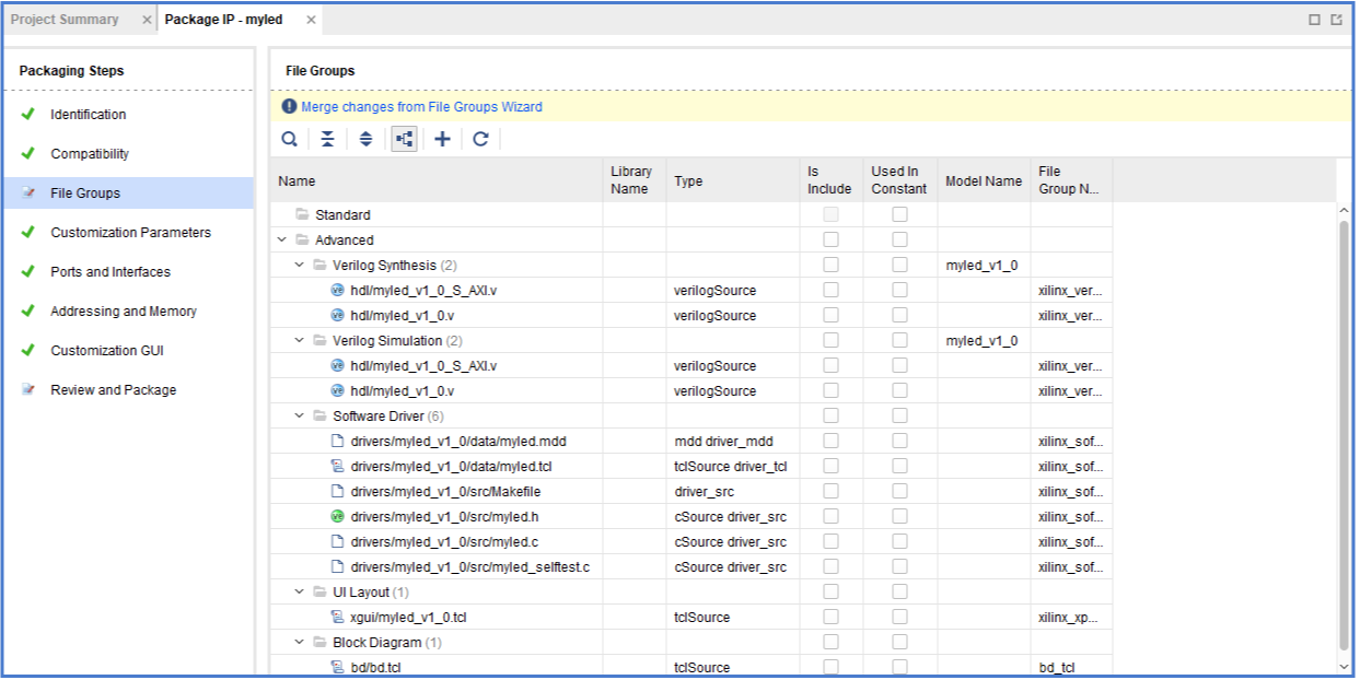
You can repackage IP with the test bench so that next time you re-create a project to edit your IP, the test bench will be saved and imported as well. To do this, go to Package IP tab and select File Groups. Click Merge changes from file groups wizard in the yellow banner.
After changes are merged to file group, you can see the test bench file hdl/myled_tb.v under folder Test Bench.
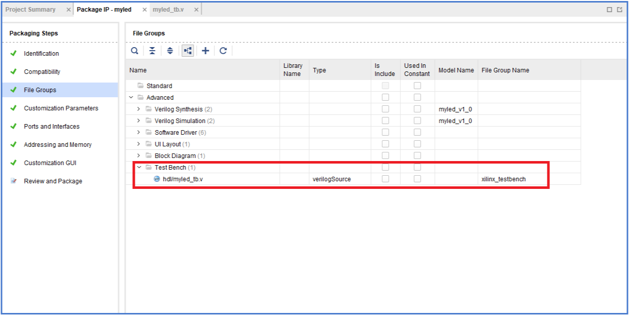
Now go to Review and Package, click Re-package IP button to write IP meta-data back to IP repository.