Zynq Processing System
Introduction to Embedded Systems: IP Cores

ZYNQ Processing System
The block diagram in figure 1 below shows the Zynq Processing System. It has many components, most of which need to be configured properly before use.
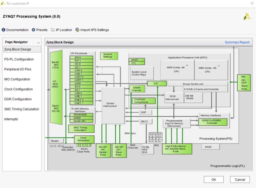
There are many peripheral controllers embedded into the processing system. The input and output pins of these controllers can be wired through predefined MIO pins, or can be routed to the programmable logic. For example, on the Blackboard, the QSPI flash is mapped to MIO 1-6, UART1 takes MIO 48 and 49, and the rest of MIO pins are connected to other controllers or the GPIO controller. Each controller has individual configurations as well. One example would be setting the baud rate of UART1 to 115200.
Besides peripheral interface controllers, the DDR memory controller needs to be properly configured and mapped to the memory space of ARM processor. Blackboard includes ISSI 46TR16256AL DDR3 memory chip that creates a single bank, 32-bit data width memory with a capacity of 512MiB. You can view the configuration of this DDR chip in the DDR configuration section.
Clock configuration of the PS system is another important aspect of setting up the Zynq system. If you open the Clock Configuration section, you can see the master clock connected to the PS system (at 33.3333Mhz). This clock is used set the frequency of all of the peripheral controllers and clocks provided to the programmable logic. The DDR controller’s clock is set to 533.33MHz, the QSPI module’s is configured at 200MHz and the first clock going to the PL(FCLK_CLK0) is set at 100MHz.
If you need furter information about the configuration of the Zynq Processing System, please refer to Xilinx’s documentation.