Basic Logic Functions and Truth Tables
Introduction to Digital Logic Fundamentals

Basic Logic Function
A digital circuit represents and manipulates information encoded as electric signals that can assume one of two voltages: logic high (Vdd) or logic low (GND). Here we will dig further into the workings of digital circuits now that you have a better foundation for understanding.
A digital circuit requires a power supply that can produce these two voltages, and these same supply voltages are also used to encode information in the form of two-state, or binary signals. Thus, if a given circuit node is at Vdd, then that signal is said to carry a logic ‘1’; if the node is at GND, then the node carries a logic ‘0’. The components in digital circuits are simple on/off switches that can pass logic ‘1’ and logic ‘0’ signals from one circuit node to another. Most typically, these switches are arranged to combine input signals to produce an output signal according to basic logic relationships. For example, one well-known logic circuit is an AND gate that combines two input signals to produce an output that is the logic AND of the inputs (i.e., if both input1 and input2 are a ‘1’, then the output is a ‘1’).
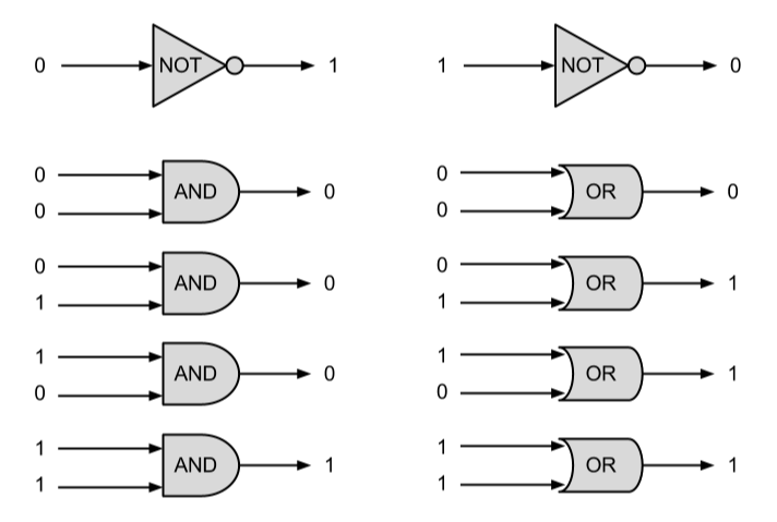
The three primary logic relationships,AND, OR, and NOT (or inversion) can be used to express any logical relationship between any number of variables. These simple logic functions form the basis for all digital electronic devices from a simple microwave oven controller to a desktop PC. We can write a collection of logic equations of the form
As engineers, we must address two primary concerns: how to express a given requirement or problem statement in terms of these simple logic relationships; and how to build electronic devices (or circuits) that can be used to implement these relationships in real devices.
Logic equations provide an abstract model of actual logic circuits. They are used to show how an output logic signal should be driven in response to changes on one or more input signals. The equal sign (’=’) is typically used as an assignment operator to indicate how information should flow through a logic circuit. For example, the simple logic equation ‘F = A’ specifies that the output signal F should be assigned whatever voltage is currently on signal A. But this does not necessarily imply that F and A are the same circuit node in fact most of the time, the use of a logic equation to specify circuit behavior implies that the inputs and outputs are separated by a circuit component.
In digital circuits, circuit components act like one-way gates. Thus, the logic equation ‘F = A’ dictates that a change on the signal A will result in a change on the signal F, but a change on F will not result in a change on A. Because of this directionality, assignment operators that indicate direction, such as ‘F = A’, are often used.
Most logic equations specify an output signal that is some function of input signals. For example, the logic equation

Compound logic expressions can be built from these basic functions. For example, an output might be need to be driven to a ‘1’ if input signals A and B are both at ‘1’ , or if input C is ‘0’, or if C is ‘1’ at the same time that A is ‘0’. This relationship can be concisely written as
Truth Tables
A truth table is the primary tool for capturing logical relationships in a concise and universally understood format. All possible combinations of inputs are shown in rows on the left of a truth table, and outputs are shown on the right. A truth table with N inputs requires

In engineering, our goal is to produce electric circuits that can implement the behavior specified for any given logic relationship. For example, a design might require a warning light to be illuminated whenever sensor A outputs a logic ‘1’, but only if sensor B also outputs a logic ‘1’ at the same time. In this example, perhaps the warning light is in an automobile dashboard, sensor A is a thermometer that outputs a ‘1’ if the temperature is above 90C, and sensor B outputs a ‘1’ if the coolant level is too low. If the coolant level ever becomes too low while the engine temperature too high, the circuit should assert its output, in order to do some work (like illuminating the warning light). We apply the same term to inputs the AND relationship in this example may be stated as the output F is asserted when the inputs A and B are both asserted.
Some input signals to logic circuits might normally be a ‘0’, changing to ‘1’ only when some input device or circuit is activated (like the push buttons on the Blackboard board). Other input signals might normally be at ‘1’, changing to ‘0’ only when an input device is activated. In either case, we can use the term asserted to indicate the input is producing a signal at either LLV or LHV in response to some action. Using this definition, an asserted signal at LHV is said to be asserted high, and an asserted signal at LLV is said to be asserted low. An asserted high signal at LLV is said to be not asserted, and an asserted low signal at LHV is said to be not asserted. The same signal definitions are also applied to output signals from logic circuits. If a logic circuit produces a LHV when its inputs are asserted, its output is said to be asserted high, and if a circuit produces a LLV at its output, the output is said to be asserted low.
Represent Basic Logic Operations in Circuits
An example of a circuit that can implement the operation
- If both switches are open, then F = VDD (or LHV);
- If one switch is open and the other closed, then F = VDD (or LHV);
- If both switches are closed, then F = GND (or LLV);

If we assume that placing VDD (or logic ‘1’) on a switch’s input causes it to close, and placing GND (or logic ‘0’) on a switch causes it to open, then we can complete a truth table that clearly shows the behavior of the circuit network under all conditions.
The series circuit can show both the AND relationship and the OR relationship: F is LLV if SW1 and SW2 are closed; and F is LHV (or VDD) if SW1 or SW2 are open. All logic circuits illustrate this property of duality, which simply means that any given logic circuit can be interpreted as performing and AND’ing relationship or an OR’ing relationship, depending on how the inputs and outputs are interpreted.
A parallel circuit can also be used to implement the function or

Note that in both cases in Fig. 5 above, the physical circuit always behaves the same way, but the behavior can be interpreted as OR-like, or as AND-like. As will be seen in later work, which interpretation is used is a matter of convenience.
Important Ideas
- The components in digital circuits are simple on/off switches that can pass logic ‘1’ and logic ‘0’ signals from one circuit node to another.
- The three primary logic relationships, AND, OR, and NOT (or inversion) can be used to express any logical relationship between any number of variables. These simple logic functions form the basis for all digital electronic devices from a simple microwave oven controller to a desktop PC.
- A truth table is the primary tool for capturing logical relationships in a concise and universally understood format. All possible combinations of inputs are shown in rows on the left of a truth table, and outputs are shown on the right.