APB Connected LED Controller
Desiging an APB LED Controller Slave and Connecting it to the Zynq Processing System

Creating An APB Peripheral
The ARM Peripheral bus is a de-facto standard used for microcontroller peripherals. Many microcontrollers and processor will have multiple buses; Typically there will one high performance bus (typically AXI or AHB) connecting the core to on chip memories and memory controllers. For connecting to peripherals such as GPIO controllers or timers, the high speed bus will be bridged into one or more slower speed ‘peripheral’ buses. Many of these peripherals don’t require the high bandwidth provided by the system main bus and by using a simpler, slower bus and bridging to the main bus, it eases the integration of peripheral IP into the larger system.
For many designs you may want to create a peripheral with an APB interface, rather than an axi interface.
The APB
Create A project for your APB IP
Create a Vivado project as usual, do not add any constraints, and select a part(this will not matter because the project will be turned into an IP project).
Define Top-Level Signals
Now define the top module for your system. The Top-level signals will be the only signals accessible when the module is packaged as an IP block. In this case we will write an APB slave, so at a bare minimum we will need the signals to interface with the APB. In our example we also add outputs specific to the peripheral.
module apb_led_ctl(

	input rst,

	//apb bus signals
	input clk,

	input [31:0] paddr,
	input psel,
	input penable,
	input pwrite,
	output pready,
	output pslverr,
	input  [31:0] pwdata,
	output [31:0] prdata,

	//led output signals
	output [7:0] led,
	output [2:0] rgbA,
	output [2:0] rgbB
);

//insantiate modules here


endmodule
Now we can write logic to go in your IP. In this case we are writing a simple set of addressable registers which hold output data. If we allocate an address to each set of outputs we will need 3 discrete addresses. To decode 3 addresses we will need 2 bits of address space: ceil(log2(n)), so our module will have 4-discrete addresses allocated to it, regardless if we use all 4. This last address could be used for an additional control register or can simply be left unused (reads return 0, writes do nothing). For now we will leave it unused.
In the code below, we create a module definition with the necessary ports and create storage elements required for our registers
module led_ctl(
	input clk,
	input rst,

	input [1:0] addr,
	input [7:0] write_data,
	output [7:0] read_data,
	input write_en,


	output [7:0] led,
	output [2:0] rgbA,
	output [2:0] rgbB
);

	reg [7:0] led_data;
	reg [2:0] rgbA_data;
	reg [2:0] rgbB_data;

	assign led = led_data;
	assign rgbA = rgbA_data;
	assign rgbB = rgbB_data;


endmodule
Write Logic
Now we can add the write decoding logic. based on the address, if the write enable signal is driven, the write_data from the bus will be stored in the corresponding register. Notice there is no logic for (addr==2’d3), as we are simply ignoring writes to this address.
	always @(posedge clk)
	begin
		//write decoding for leds
		if(rst)
			led_data<=8'd0;
		else if(write_en & (addr==2'd0) )
			led_data<=write_data;

		//write decoding for rgbA
		if(rst)
			rgbA_data<=2'd0;
		else if(write_en & (addr==2'd1) )
			rgbA_data<=write_data[2:0];

		//write decoding for rgbB
		if(rst)
			rgbB_data<=2'd0;
		else if(write_en & (addr==2'd2) )
			rgbB_data<=write_data[2:0];
	end
Read Logic
For the read logic, we only need combinatorial logic. Based on the address, we can drive the data bus with the appropriate register data. Unlike the write logic, we need to cover for unused addresses (something always needs to be driven on the read data bus).
	reg [7:0] in_rdata;
	assign read_data = in_rdata;

	always @(*)
	begin
		case(addr)
			0:
				in_rdata= led_data;
			1:
				in_rdata = {5'd0,rgbA_data};
			2:
				in_rdata = {5'd0,rgbB_data };
			3:
				in_rdata = 8'd0;
		endcase
	end
Instantiating logic and connecting to the APB.
Now we can instantiate our controller module and wire it up to the APB. The APB provides a 32-bit address space, however our module has only 2 bits of address necessary. If we map the two-lowest bits of the address,
Take care when assigning address bits. The ARM’s address space is byte-addressed, meaning every discrete address is (). The Zynq only allows 32-bit aligned accesses to the programmable logic, so you need to insure your registers are addressed on 32-bit boundaries (address is a multiple of four). This is easily accomplished by assuming the lowest 2 address bits will be zero, and using only higher order bits in addressing.
For driving the pready signal, we can tie it high; Our module has no need to extend any transactions. Similarly pslverr can be tied low, as no cases exist for needing an error condition.
The write enable signal to your registers should be driven when the slave is selected, the transaction is in the access phase (penable is 1), and the transaction is a write (pwrite is 1).
module apb_led_ctl(

	input rst,

	//apb bus signals
	input clk,
	input [31:0] paddr,
	input psel,
	input penable,
	input pwrite,
	output pready,
	output pslverr,
	input  [31:0] pwdata,
	output [31:0] prdata,

	//led output signals
	output [7:0] led,
	output [2:0] rgbA,
	output [2:0] rgbB
);

	wire write_en;
	wire [1:0] addr;

	//IMPORTANT, make sure you don't use bits [1:0]
	assign addr = paddr[3:2];
	assign write_en = (psel & penable & pwrite);

	assign pready=1'b1;
	assign pslverr=1'b0;


	led_ctl led_inst(
		.clk(clk),
		.rst(rst),
		.addr(addr),
		.write_data(pwdata[7:0]),
		.read_data(prdata[7:0]),
		.write_en(write_en),

		.led(led),
		.rgbA(rgbA),
		.rgbB(rgbB)
	);

	//make sure remaining data bits are driven
	assign prdata[31:8]=0;


endmodule
Creating an IP Project
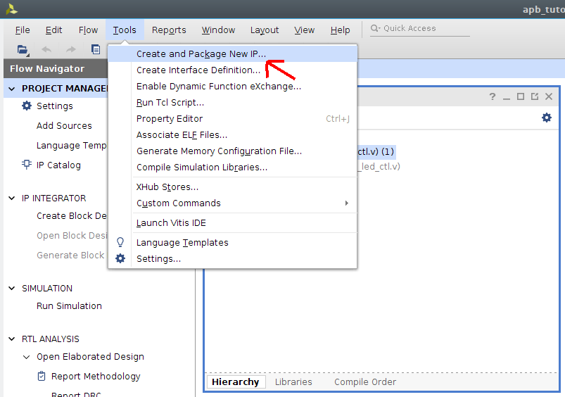
Now we can package our module as an IP. Select Tools->create and package new IP, this will open a dialogue to configure your IP.
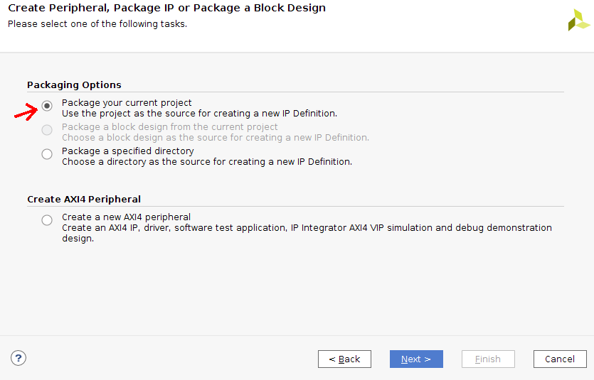
In ‘Packaging Options’ select “Package your current Project”. In the next dialogue you will be asked for a location for your IP. You can place it in the default location, or move it elsewhere. Either way, make sure you can find this location later. Complete the wizard’s steps and Vivado will open a new IP project.
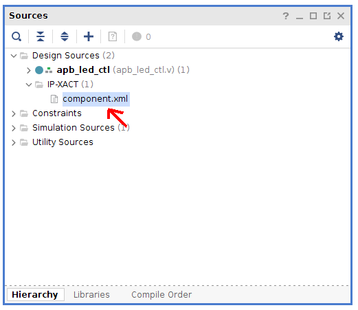
In an IP project you can edit your HDL as usual but also configure how your IP will be packaged. To do this, open up the IP-XACT folder and click on “component.xml”. This will bring up the options for packaging your IP.
Defining the APB interface and mapping signals to it
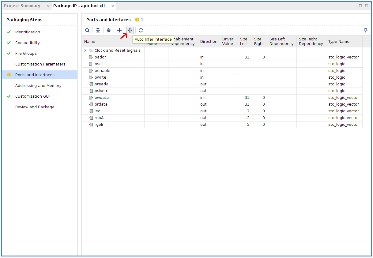
To make for easy connection in the block design, we can add an ‘apb’ interface to our IP. Open the ‘ports and interfaces’ tab. In here you will see the top-level signals of your module. Select “auto-infer interface”.
In the dialog select Advanced->apb_rtl.
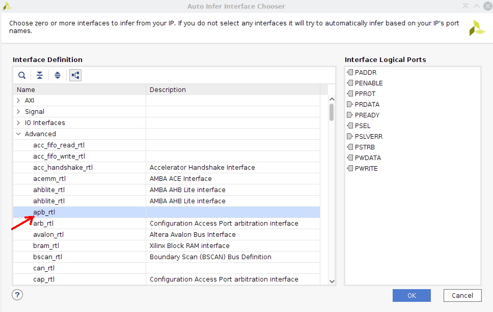
This should create an apb subgroup in your port list, and automatically add apb signals to it (It does this based off of the signal’s name, so you need to be careful when defining top level signals).
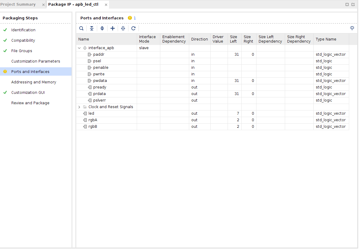
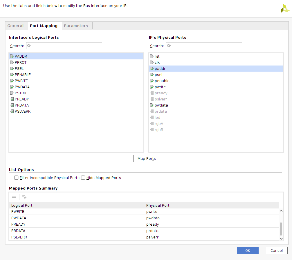
If not all of your apb signals are mapped, you can open the port-mapping tool and manually map the remaining ports. In the port mapping screen you can also confirm the ports have been mapped correctly to the APB interface.
Configuring Addressing
The block design tool in Vivado can map the address space of slaves into the address space of a bus master such as the Zynq’s ARM Processor. In the IP packager, a logical interface needs to be given an address block so the block design tool knows how to map the slaves addresses. This does not affect how the core is synthesized, but it does affect how the bus it is connected to is configured. In the IP packager select the ‘Addressing and Memory’ Tab, and run the Addressing and Memory Map Wizard.
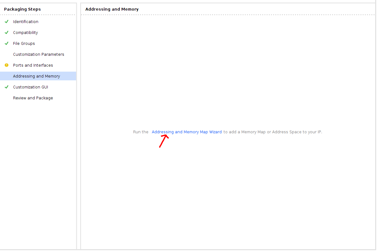
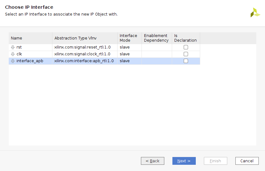
Select the APB interface and give it a name. Click next and then finish.
Now your interface will show up in the Addressing and Memory pane. Right click on the interface and select “add address block”.
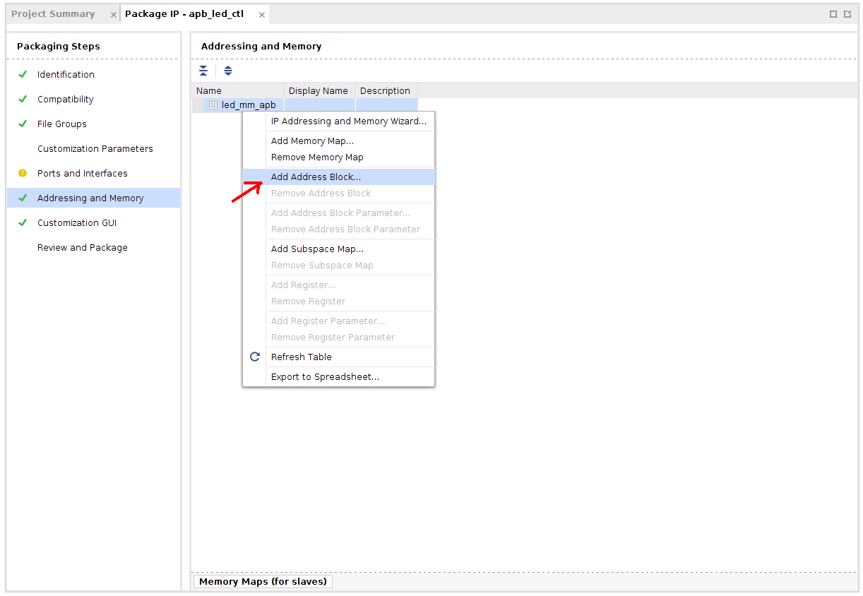
In the address block you can modify the properties of the IP’s address space. In our case we have 4-accessible 32-bit addresses, which is 16 memory locations for the ARM (though only 4 will be accessed). Set range to 16. For IP cores that need more memory space this can be modified (The Minimum range should at least cover any addressable memory, but can be greater).
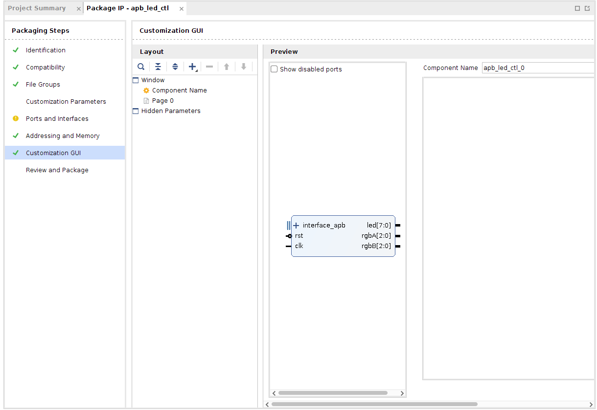
Customization GUI
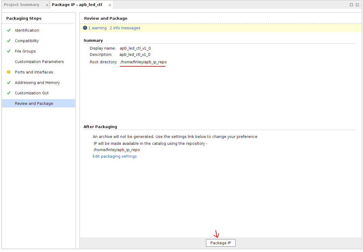
Now you can open the ‘customization GUI’ tab. Here you can verify the ports and interfaces available on your IP. If everything looks correct, you can move on to ‘Review and Package’ where you can package your IP as a self-contained unit.
After you click “package IP” Vivado will tell you where to find your IP. Make sure you remember this location so you can add it to your IP catalog.
Add your IP to a block design
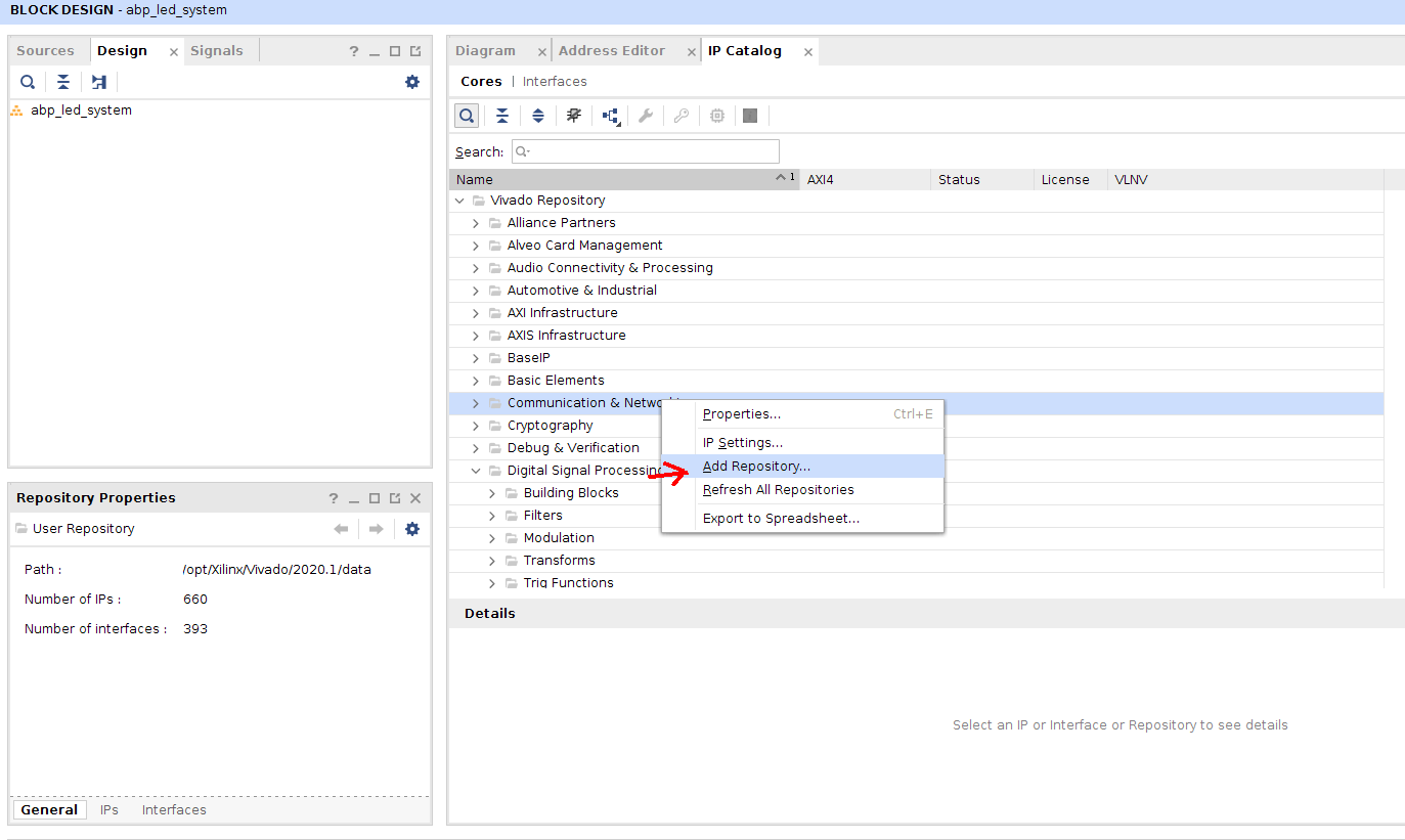
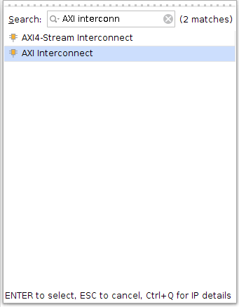
Now you can create a project for your Zynq system block design. Once you have created your project, Open the IP Catalog. Right click and select “add repository”. Navigate to the location you packaged your IP and select the folder. Now in the block design you can add your IP block.
Adding your IP to the block Design
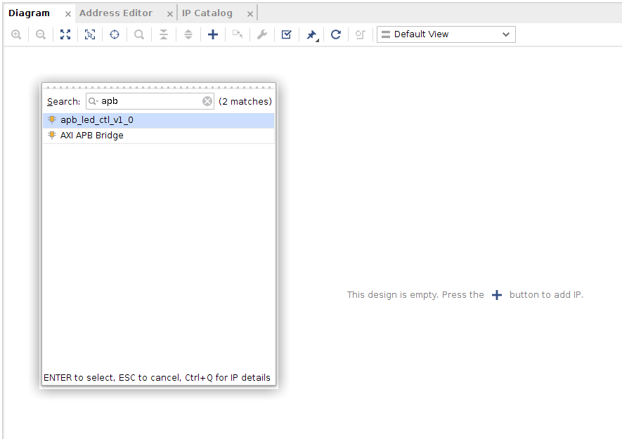
Once your IP repository is added, you can find your IP in the IP catalog and add it into a block design
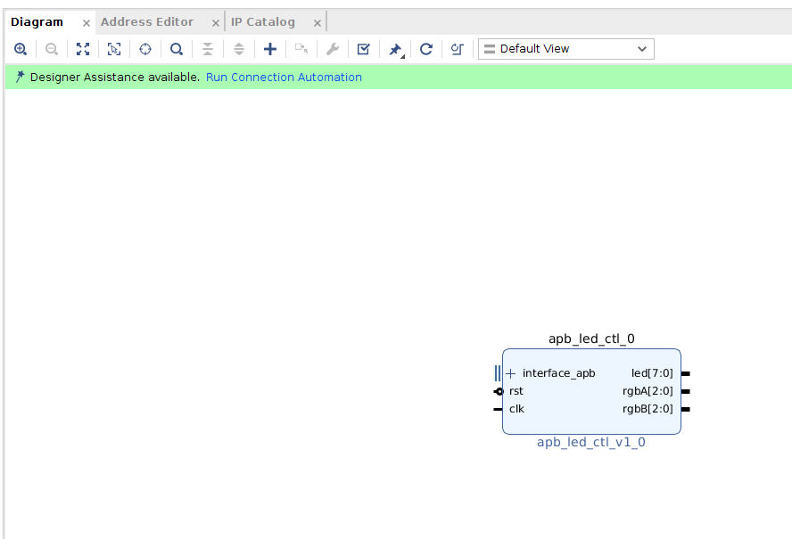
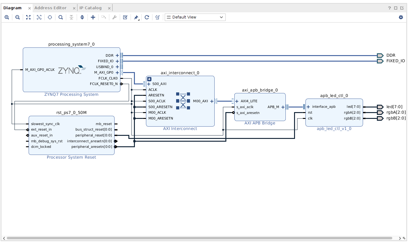
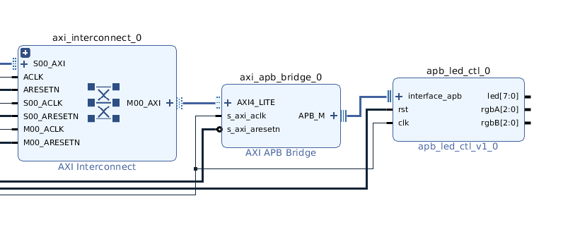
Connecting your IP to the Zynq Processing system
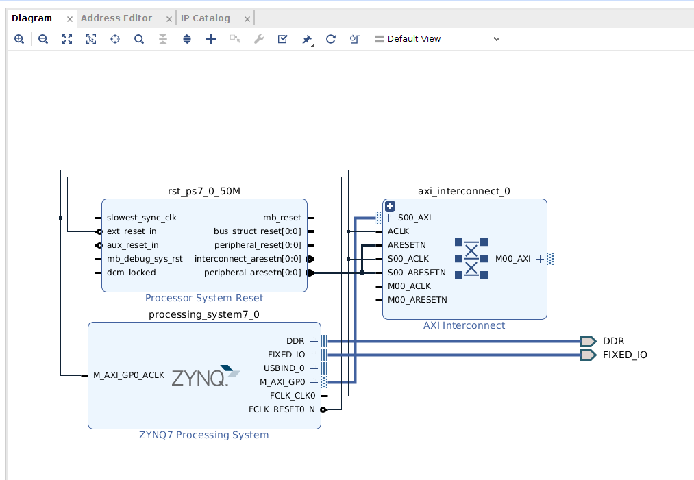
If you haven’t already added a Zynq IP block to your design, do so now. Make sure to apply the correct presets file and run block automation. Since the Zynq has AXI ports you will need to add an axi bridge to your system. If your design does not already have an AXI interconnect, add one to your design.
Make sure the Master port and clocks of the Zynq are connected properly to the interconnect.
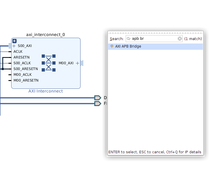
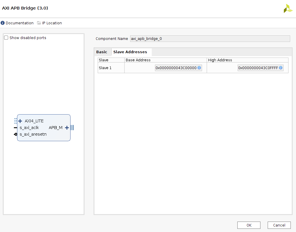
Now add an AXI-APB bridge and connect it to one of the interconnect’s master ports.
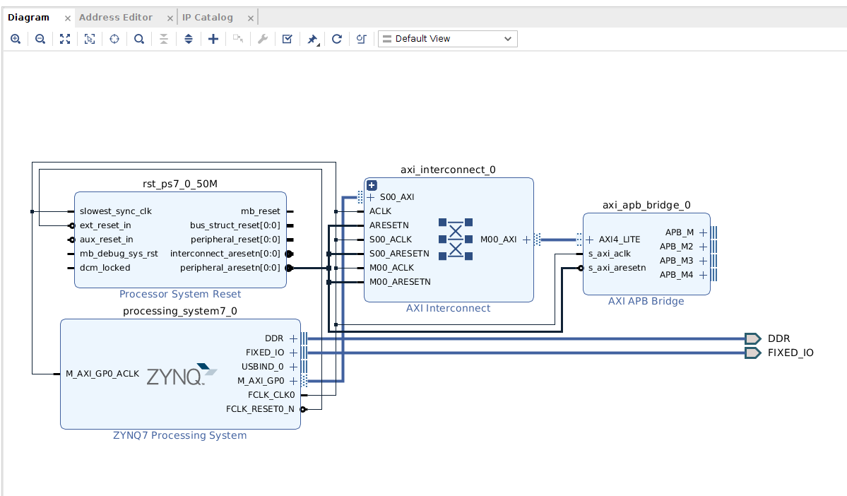
You can now connect your apb ip to the bridge. Make sure to connect your module’s clock to the same clock as the bridge and a reset of the correct polarity. You can configure the AXI-APB bridge for additional slave ports, should you need more. You can also reduce the number of Available ports.
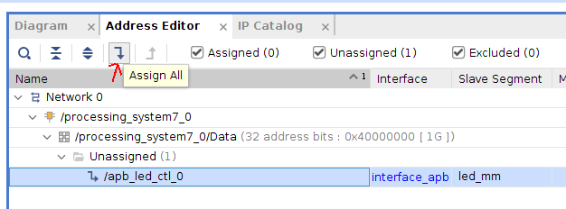
Mapping an APB Slave
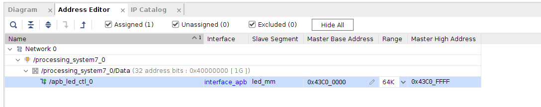
Once Connected to the Zynq system, you can map the slave into the address space of the processor. Open the Address Editor tab. Here you should see the apb ip is in the category of ‘unmapped slaves’. To map it into the processor’s address space, select the ip and click on “auto assign address”.
This will give the IP a base address and a range. Any accesses in this address space from the processor will drive the ‘psel’ for that peripheral high.
Now click Validate Design. If any errors pop-up you will need to correct them.
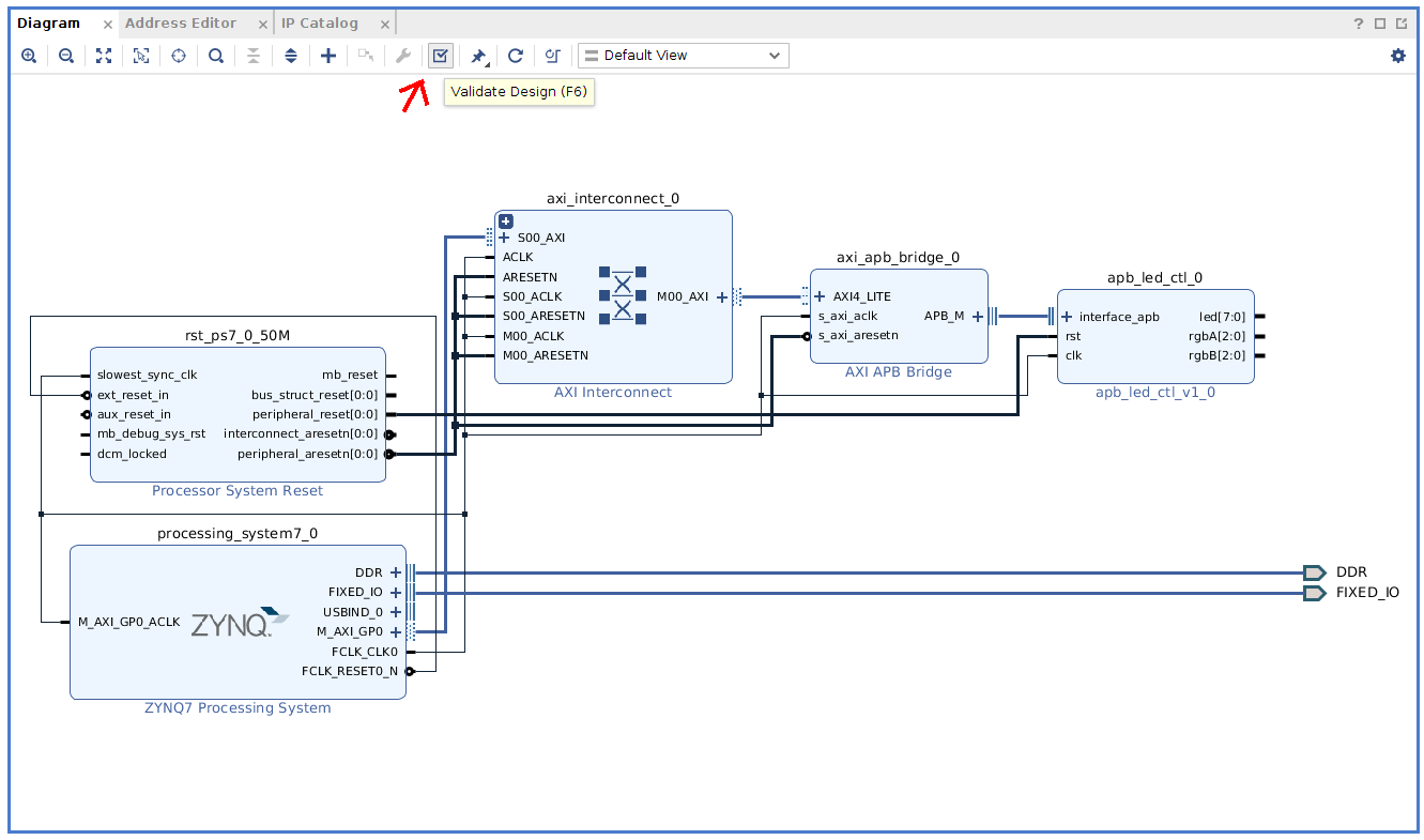
Once you have validated your design, you can verify the address you mapped to your slave device by opening the configuration page for the AXI-APB bridge. (Changes to the Bridge’s Addressing are made when the design is validated)
Complete Your block design
Now you can complete your system’s block design and connect any necessary inputs and outputs. Once you generate a bitstream you can export the hardware to Vitis where you can write a software program. From a software viewpoint, any APB slave is accessed the same as an AXI IP (using loads and stores to memory).