Configuring ZYNQ7 Processing System
Setting up Zynq Processing system to use SPI,I2C, and UART modules

ZYNQ7 Processing System Configuration
This short tutorial will walk you through on how you can configure ZYNQ7 processing system so that MIO pins would be used for certain peripherals, such as SPI,I2C, and UART.
Setting up MIO pins for I2C, SPI, and UART
Open up ZYNQ7 Processing System by double clicking on the IP block.
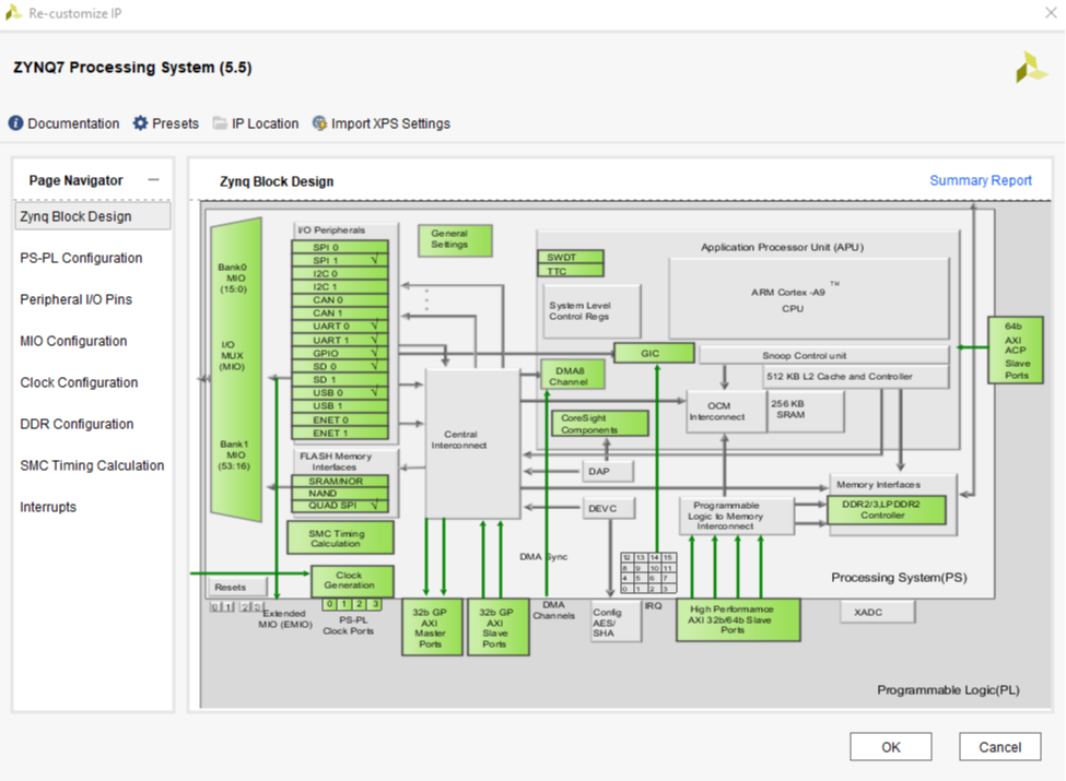
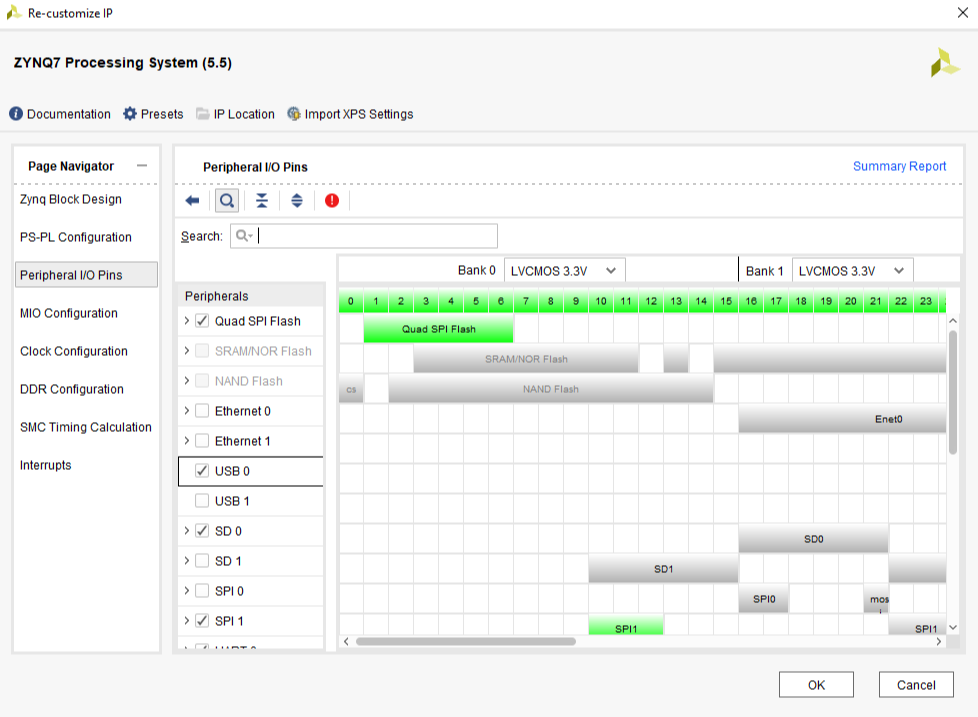
Click on Peripheral MIO Pins. You will then see a window as show in figure 2, where some peripherals are already configured and other’s aren’t.
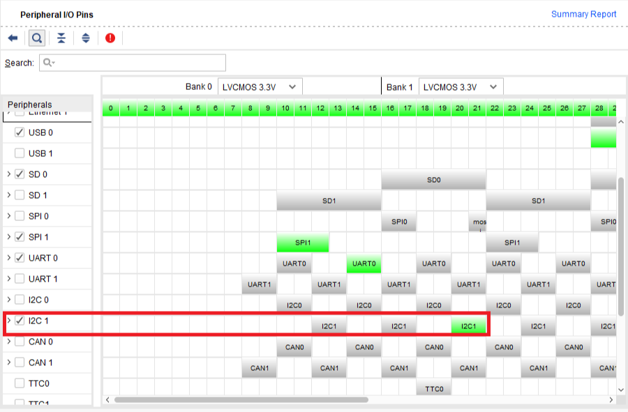
Step 1: I2C1 Configuration
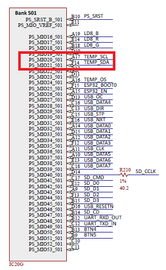
In order to configure the I2C MIO pins, you need to find out on what pins the I2C bus is connected to. From figure 3, you can see that TEMP_SCL and TEMP_SDA are connected to MIO pins 20 and 21, respectively. You can also see from the figure that TEMP_OS (interrupt signal) is connected to MIO pin 24.
Use the top array of MIO pin numbers to find the correct pins for the I2C as shown in figure 4. You will notice that there is only one I2C bus (I2C1) under MIO pins 20 and 21.
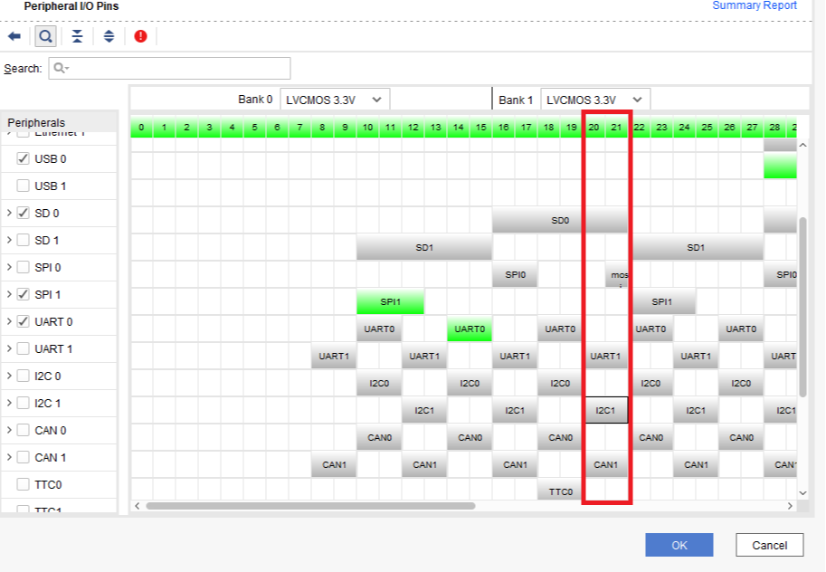
Click on I2C1 button as shown in figure 5 (The button should turn green).
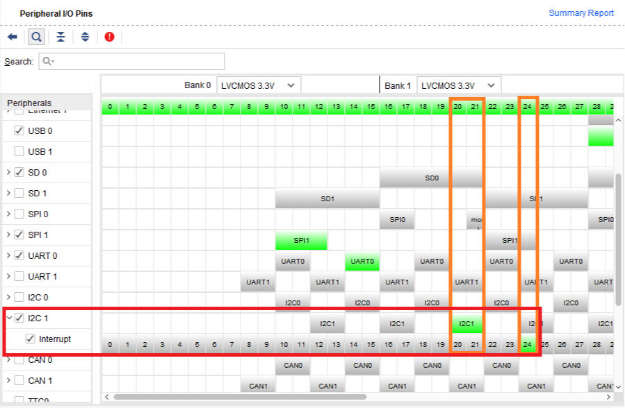
Click on the small arrow on the I2C 1 peripheral to configure the interrupt under MIO pin 24.
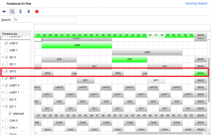
Step 2: Configuring SPI0 bus as an EMIO
Since SPI0 pins can only be connected through the FPGA, you need to configure SPI0 as EMIO (External MIO). This functionality simply enables you to use the SPI0 bus in the ZYNQ7 processing system through the FPGA. Click on the EMIO button in the end of the SPI0 line to enable the EMIO pins. Later on you will make the connections to the FPGA from the block design (.XDC file).
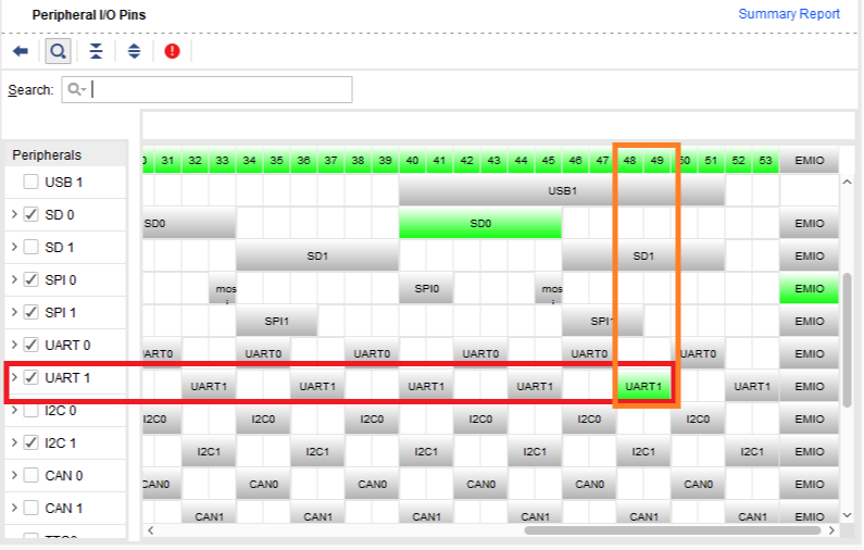
Step 3: UART1 Configuration
In order to configure the UART MIO pins, you need to find out on what pins the UART bus is connected to. From figure 8, you can see that UART_RXD_OUT and UART_TXD_IN are connected to MIO pins 48 and 49, respectively.
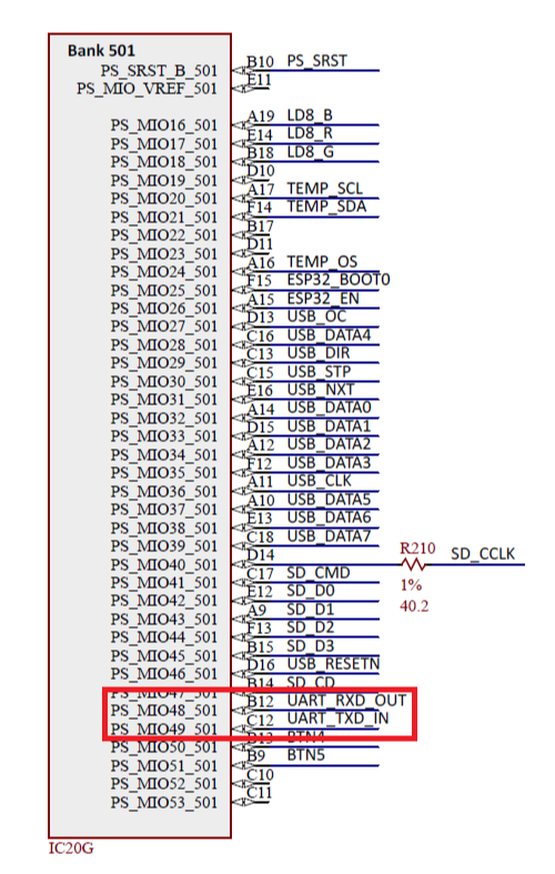
Locate UART 1 pins 48 and 49 like you did for I2C. Click on the UART1 button as shown in figure 9 to configure the MIO pins 48 and 49 to be used as UART1.
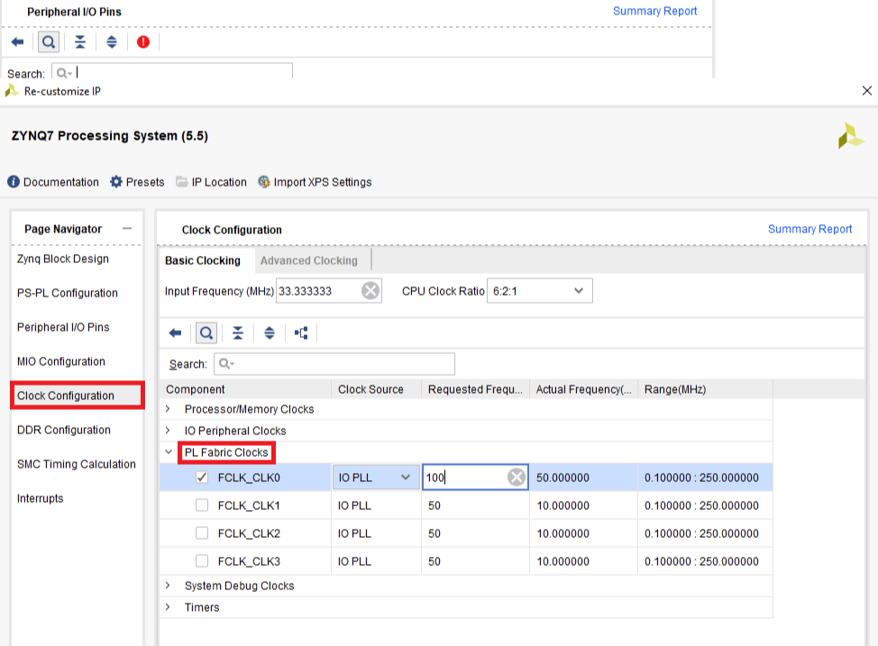
Step 4: Configure FCLK_CLK0 Clock Frequency
Click on Clock configuration and then on PL Fabric Clocks. Change the FCLK_CLK0 frequency to 100MHz as shown in figure 10. The FCLK_CLK0 is ued to determine the frequency for the AXI interface.
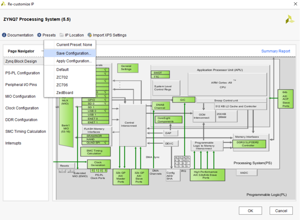
Step 5: Save Configuration for Future Use
Click on Presets and then choose Save Configuration…. Choose a desired location to save the new configuration as a .tcl file that you can possibly use for future projects. After you’ve saved the configuration, press OK.
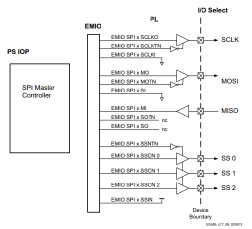
Step 6: Finish SPI0 Configuration
To configure SPI Master Controller through EMIO pins, you need to follow the diagram in figure 12. (Figure 12 is acquired from UG585-Zynq-7000-TRM under SPI Section; figure 17-8).
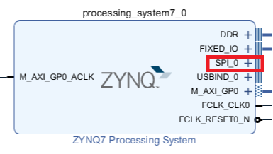
You’ll notice that your ZYNQ7 IP block has changed. Click on the + sign right next to SPI0 as shown in figure 13.
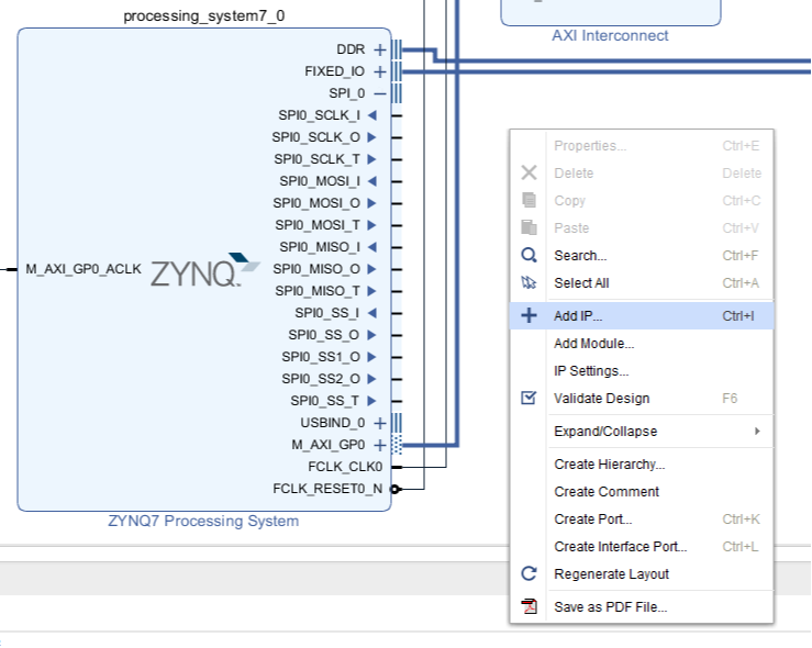
Right click anywhere on the white space and press Add IP…
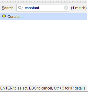
Search for Constant as shown in figure 15 and click on it.
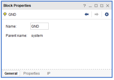
Constant IP core has been placed to your block design. Next, change the name of this IP Core in your block diagram by clicking once on the IP Core and you will see a diagram in the bottom left named Block Properties.
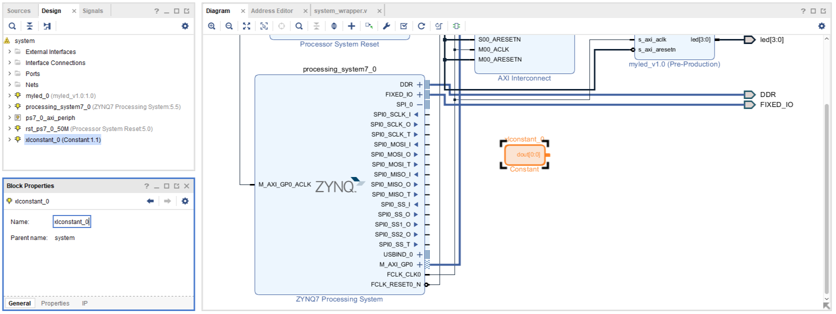
Change the name to GND from the block properties.
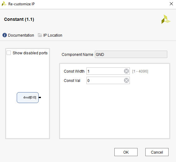
Now double click on the IP block GND. Change the Constant value to 0.
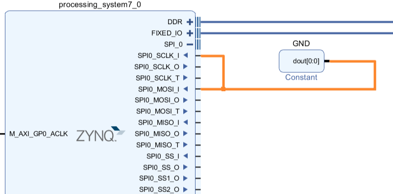
Connect dout of the GND block as shown in figure 19 to the SPI0 EMIO pins.
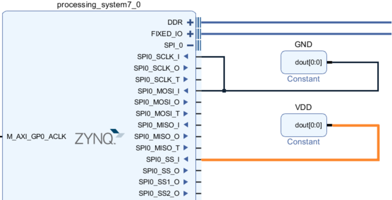
Add another Constant IP Core and name it VDD. Make sure that the constant value is 1. Then connect it to the rest of the system as shown in figure 20.
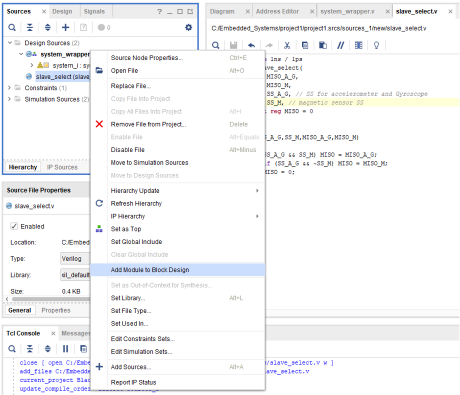
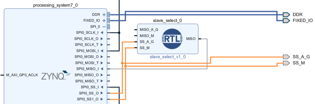
Since there is only one MISO line under the SPI0 EMIO pins and two MISO lines for the NAV sensor, you need to create a module that would choose the correct MISO line for data transfer based on the correct Slave Select Line. Create a new module under design sources and name it slave_select. Copy the following code to the new module you created.
`timescale 1ns / 1ps
module slave_select(
    input MISO_A_G,
    input MISO_M,
    input SS_A_G, // SS for accelerometer and Gyroscope
    input SS_M, // magnetic sensor SS
    output reg MISO = 0
    );

always@(SS_A_G,SS_M,MISO_A_G,MISO_M)
begin
    if (~SS_A_G && SS_M) MISO = MISO_A_G;
    else if (SS_A_G && ~SS_M) MISO = MISO_M;
    else MISO = 0;
end
endmodule
Right click on the module you created (slave_select) and choose Add Module to Block Design.
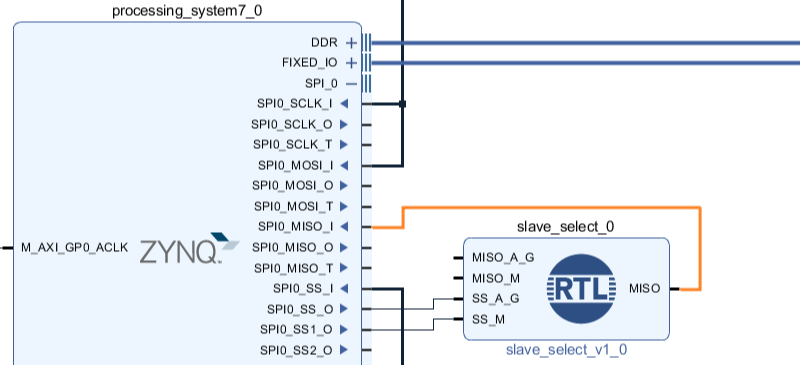
Connect the MISO, SS_A_G, and SS_M lines to the ZYNQ7 Processing System as shown in figure 22.
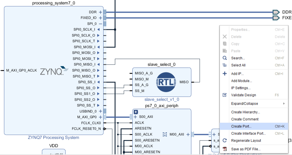
Right click anywhere on the white space and select Create Port.
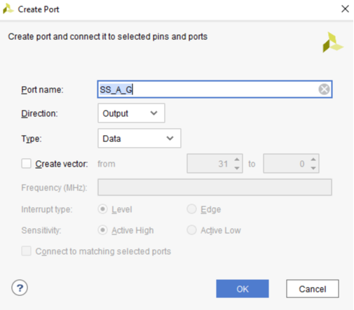
Create Port Dialog will appear. Name the port as SS_A_G, set the direction as Output, and type as data. Press OK
Create another port named SS_M similar to how you created SS_A_G. Connect these ports to the rest of the system as shown in figure 25.
Next, create appropriate ports for MISO_A_G, MISO_M, SPI0_SCLK_O, and SPI_MOSI_O. Finish your design by updating the constraints .XDC file for the SPI0 bus.
Where to find information about I/O Constraints
You can find the location you need from the Blackboard, or you can download the Blackboard master XDC for your board from the Real Digital®’s website and copy the corresponding lines for this step.