Cascade Clock Dividers
Basic Cells of Sequential Circuits

Step 1: Implement D-FF in Verilog
In this step, you are going to implement a D-FF with asynchronous reset.
Declare DFF Module
As the block diagram in Fig. 1 shows, D flip-flops have three inputs: data input (D), clock input (clk), and asynchronous reset input (rst, active high), and one output: data output (Q).
module dff(
    input D,
    input clk,
    input rst,
    output Q
);
Describe DFF Behaviorally
To describe the behavior of the flip-flop, you are going to use an always block. On the contrary to combinational circuits, the output of flip-flop changes when a rising edge or falling edge of clock occurs or the reset is asserted. In other words, output Q is sensitive to clock signal clk and reset signal rst. So you can describe the circuit as follows: always at rising edge of clk or rising of rst, if rst is asserted, Q is driven to logic ‘0’, else Q is driven by D. In Verilog code:
always @ (posedge(clk), posedge(rst))
begin
    if (rst == 1)
        Q <= 1'b0;
    else
        Q <= D;
end
Check your Verilog File
So the final Verilog implementation of a D-FF looks as follows:
`timescale 1ns / 1ps
module dff(
    input D,
    input clk,
    input rst,
    output Q
    );

always @ (posedge(clk), posedge(rst))
begin
    if (rst == 1)
        Q <= 1'b0;
    else
        Q <= D;
end

endmodule
Step 2: Implement the Clock Divider to Blink an LED
The block diagram of the clock divider is shown in Fig. 4. Name the internal wire out of the flip-flop clkdiv and the wire connecting to the input of D-FF din. The frequency of each clkdiv is shown in red.

Declare Clock Divider
In this design, you need two inputs: on-board clock input clk, and a push button as reset signal rst. You have one output to blink an LED, so let’s call it led.
module clk_divider(
    input clk,
    input rst,
    output led
    );
Declare Internal Signals
You need to declare all the internal wires you are going to use.
wire [26:0] din;
wire [26:0] clkdiv;
Describe Clock Divider Structurally
We need to instantiate 27 flip-flops with 27 inverters to divide the clock frequency by
dff dff_inst0 (
    .clk(clk),
    .rst(rst),
    .D(din[0]),
    .Q(clkdiv[0])
);
For the rest 26 flip-flops, you can copy the code above 26 times and change the names of the internal wire each port will map to. However, we can also use generate statement with a for loop in Verilog to generate the code for us. By observing the block diagram shown above in Fig. 3, starting from the second flip-flop, rst port of D-FF is always connected to signal rst. If the port D is connected to signal din[i], then clk port is connected to clkdiv[i-1] and Q port is connected to clkdiv[i]. So, we can generate the 26 D-FFs:
genvar i;
generate
for (i = 1; i < 27; i=i+1)
begin : dff_gen_label
    dff dff_inst (
        .clk(clkdiv[i-1]),
        .rst(rst),
        .D(din[i]),
        .Q(clkdiv[i])
    );
    end
endgenerate;
We can use the same generate statement to instantiate 27 inverters, or by observing the connections, the bus din is actually the inverse of bus clkdiv. So, instead of writing the generate statement, we can simply write one assign statement as follows:
assign din = ~clkdiv;
Connect the output of the flip-flop in the final stage to led.
assign led = clkdiv[26];
Check your Code
Verilog file of the design should be as follows:
`timescale 1ns / 1ps
module clk_divider(
    input clk,
    input rst,
    output led
    );

wire [26:0] din;
wire [26:0] clkdiv;

dff dff_inst0 (
    .clk(clk),
    .rst(rst),
    .D(din[0]),
    .Q(clkdiv[0])
);

genvar i;
generate
for (i = 1; i < 27; i=i+1)
begin : dff_gen_label
    dff dff_inst (
        .clk(clkdiv[i-1]),
        .rst(rst),
        .D(din[i]),
        .Q(clkdiv[i])
    );
    end
endgenerate;

assign din = ~clkdiv;

assign led = clkdiv[26];

endmodule
Step 3: Create a Simulation Test Bench and Simulate the Clock Divider Circuit
As with the combinational circuit we have designed in previous projects, you can draft a test bench to test the circuit out before implementing it on-chip. However, in this test bench, we need to emulate the clock signal and the rst signal. The clock signal is actually a constantly oscillating signal. Using the Blackboard as an example, the input clock frequency is 100 MHz, i.e., the period of the clock is 10 ns. Half of the period the clock is high, half of the period clock is low. In other words, every half of the period, 5 ns in this case, the clock will flip itself. To simulate the clock signal, instead of putting it in the initialize statement, we will use an always statement.
`timescale 1ns / 1ps

...

reg clk;

always
    #5 clk = ~clk;
In the initialize block, we will initialize clk signal to 0 and hold rst high for 10ns to reset the clock divider. So, the Verilog Test Bench will look like this:
`timescale 1ns / 1ps

module tb;

    // Inputs
    reg clk;
    reg rst;

    // Outputs
    wire led;

    // Instantiate the Unit Under Test (UUT)
    clk_divider uut (
        .clk(clk),
        .rst(rst),
        .led(led)
    );

    always
        #5 clk = ~clk;

    initial begin
        // Initialize Inputs
        clk = 0;
        rst = 1;

        #10 rst = 0;

        // Wait 100 ns for global reset to finish
        #100;

    end

endmodule
Simulating the Clock Divider
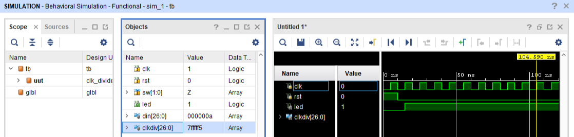
When you first run behavioral simulation, the internal signals such as clkdiv[26:0] won’t appear in the simulation window. You can access these signals by opening windows Scope and Objects on the left side of the simulation window and clicking on uut under Scope window. Now you can see clkdiv[26:0] under Objects window, go ahead and click and drag this signal to the simulation window under the Name column as show in figure 3. You can also drag clkdiv[26:0] signals into the simulation window one by one in any order you want.
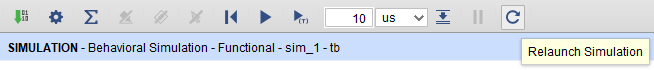
Now you have clkdiv[26:0] in your simulation window, but it doesn’t have any signals. In order to see those signals, you need to relaunch your simulation by clicking Relaunch Simulation icon  as shown in figure 4. You can also achieve the same result by clicking on Restart icon
  to restart the simulation and then clicking on Run All icon
  to start the simulation again, both of which can be found on the same toolbar as the Relaunch Simulation icon.
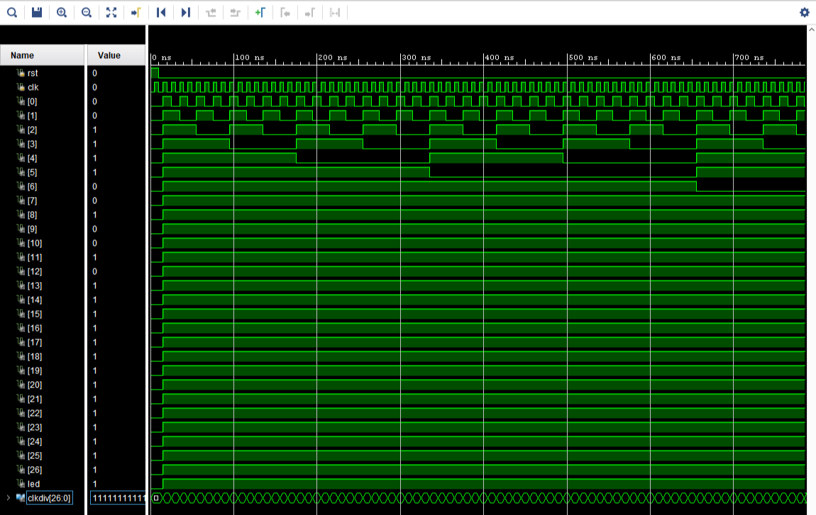
The simulated waveform is shown in Fig. 5 below. You can see in the waveform that clkdiv[0] is half of the frequency of clk, and that clkdiv[1] is half of the frequency of clkdiv[2].