Using the Integrated Logic Analyzer
Capturing Data using a design connected to a ChipScope ILA

Introduction
This document will cover the use of the Xilinx Integrated Logic Analyzer. It is a follow up to the document “Setting up Integrated Logic Analyzer”, which covers how to connect chipscope probes to the design’s signals. The previous document also contains the example module used in both tutorials. This tutorial will cover opening the chipscope display, adding wires to the waveform monitor, and setting up triggers to capture data.
Program your Design and Connect to the ILA Core
Open the Hardware Manager and connect to your board. Click on ‘Program Device’. In the dialogue you should see both a bitstream file and a ‘Debug Probes File’. If you don’t see the debug probe file you will have to find it within the project directory structure. The file has the extention of ‘.ltx’ (lowercase l) it should have the same name and be in same location as your bitstream (Usually it can be found in your project’s runs folder, under the most recent implementation directory). Once you have a bitstream and debug file shown, program the device with the bitstream.
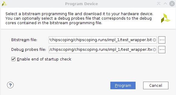
After programming, if the hardware manager displays ‘there are no debug cores’. go through the steps in the previous tutorial and make sure your synthesized design shows an ILA core in the schematic view. When programming the bitstream, make sure the debug probe file (.ltx) is also programmed. If the debug window still does not appear try changing the JTAG communication speed using the procedure below.
Note about JTAG Communication and Clock speeds
The ChipScope ILA is accessed through the same JTAG interface used to program the FPGA. On Zynq platforms JTAG is also used to debug the ARM cores in the Zynq PS. In fact, the JTAG is interfaced as a ‘chain’ of devices all linked together and looped back to the host device. In the hardware manager you can see the different JTAG-connected devices in the ‘scan-chain’.
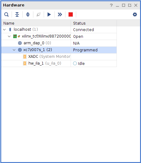
In the figure you can see there is one hardware target with two devices, the ARM core found in the Zynq, as well as the Programmable Logic section of the Zynq (the FPGA). In the programmable logic there are further items in the chain, the XADC system monitor, and the ILA core which was instantiated in the previous tutorial. If you are having trouble connecting to the ILA core, or experience strange behavior, for example triggers refusing to arm, you may need to reduce the JTAG communication speed to the device.
By default, the JTAG-USB interface on the blackboard is configured to communicate with the Xilinx device at 15MHz. If devices on the scan chain cannot operate at this speed, they may not be able to communicate properly with the through the connection. In the case of the ChipScope ILA, if the clock running the ILA (the associated clock domain in ‘set up debug’) is lower than the JTAG communication rate, the ILA core will be unable to communicate properly through the JTAG interface. Xilinx recommends the JTAG speed be 2.5 times slower than the slowest device in the scan chain.
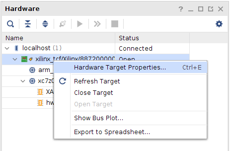
To set the communication rate with the Xilinx chip, in hardware manager, right click the hardware target and select ‘hardware target properties’.
In the properties window, open the ‘PARAM’ drop down menu to find ‘FREQUENCY’ This value is in Hz. Set this to a value at least 2.5x slower than your ILA’s input clock.
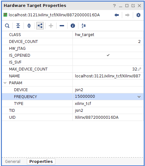
Note: This will affect the speed of ALL devices in the JTAG scan chain. Tasks like programming the FPGA or uploading ARM code to DDR will take longer than at the default speed (you will notice it you select a much slower frequency than the default). If you are no longer using the ILA, it is a good idea to reset the frequency to 15MHz.
The Waveform Display
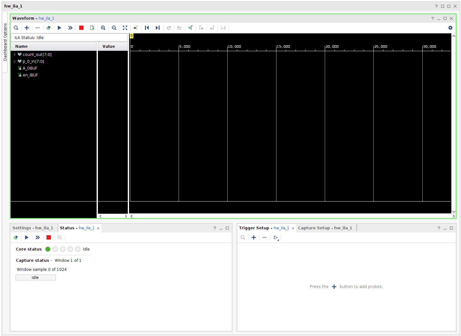
You should now have the ILA Waveform display view open. If you have programmed your board and exited the hardware manager, you can access the waveform display by opening the hardware manager and connecting to the programmed device. The waveform display looks similar and has many of the same features as the Vivado simulator’s waveform display. By default, some of your probed signals will be added to the display. Below this you should also see the core status and trigger setup windows. If you do not see any of these panels you can enable them through the dashboard options menu.
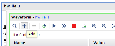
If you need to add any signals to the display click the “Add Probes” icon.
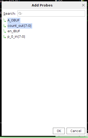
In the dialogue select any signals you want to add to the display.
Note: You can rename signals in the waveform display window by double-clicking on the name field, This might be helpful for a larger number of signals, or if the given names are not intuitive.
Capturing Data Immediatly
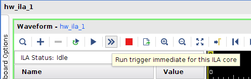
To view runtime data from the ILA, you will have to have ‘trigger’ a data capture. You can do this immediately by pressing the “Run Trigger Immediate” button.
Once you capture data, it will show up on the waveform display. The trigger time will be represented by the red line with a red ‘T’ box above it. By default there is data collected before and after the trigger.
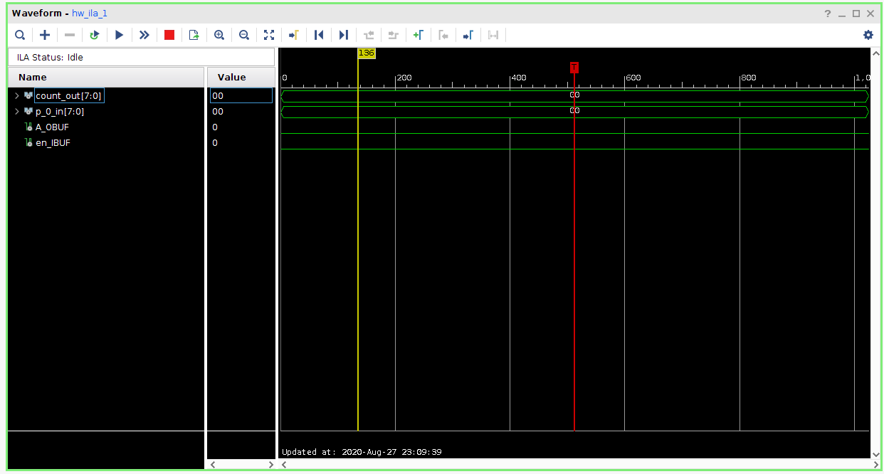
In the example the trigger shows up at sample 512, the halfway point between sample 0 and sample 1023. Since the counter in the example module only runs when enabled and the output goes high only when switch value is non-zero, the signals do not show change.
Configuring and Arming Triggers
Using trigger immediate can give you an instantaneous snapshot of your circuit’s operation, but it can be hard to find a specific occurance of behaviour when using it. Setting up a trigger will allow you to capture data when a specifc event happens.
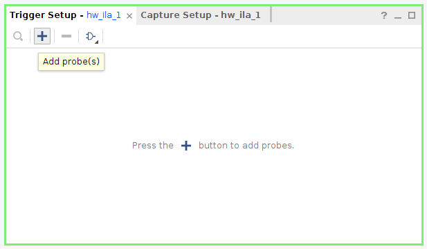
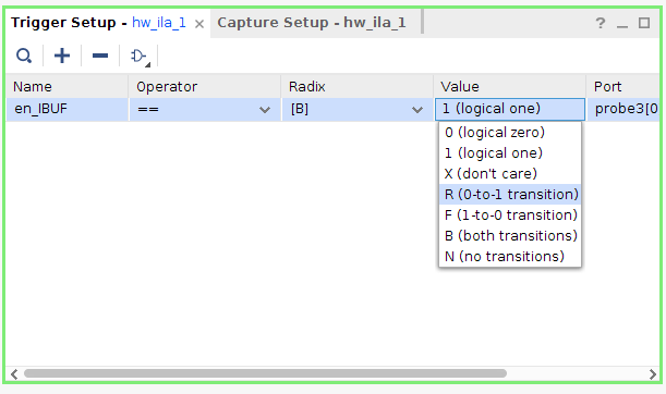
In the trigger setup window you can add a trigger to the ILA using the “Add Probe(s)” button
In the “Add Probes” menu, select the signal or bus you will use as a trigger. Here, selecting a signal or bus it will place it in trigger setup window. In the example the binary counter’s enable signal was added to the triggers list.
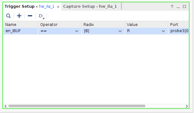
The value and operator fields in the menu are used to set the event which the trigger is based off of. For a single wire this the value can be an edge transition or based on the signal level (‘high or low’). For a bus, the value field must be based on the value of the wire. Whenever the trigger condition is met and the ILA core is armed, data will be captured.
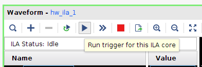
Once there is at least one trigger configured, the ILA can be armed by clicking the “Run Trigger” button in the waveform display. Once pressed, the core status will change to “Waiting for Trigger”. The core will remain in this state until either the trigger event occurs, or the core is disarmed.
When the event occurs, The waveform display will update to show the captured data.
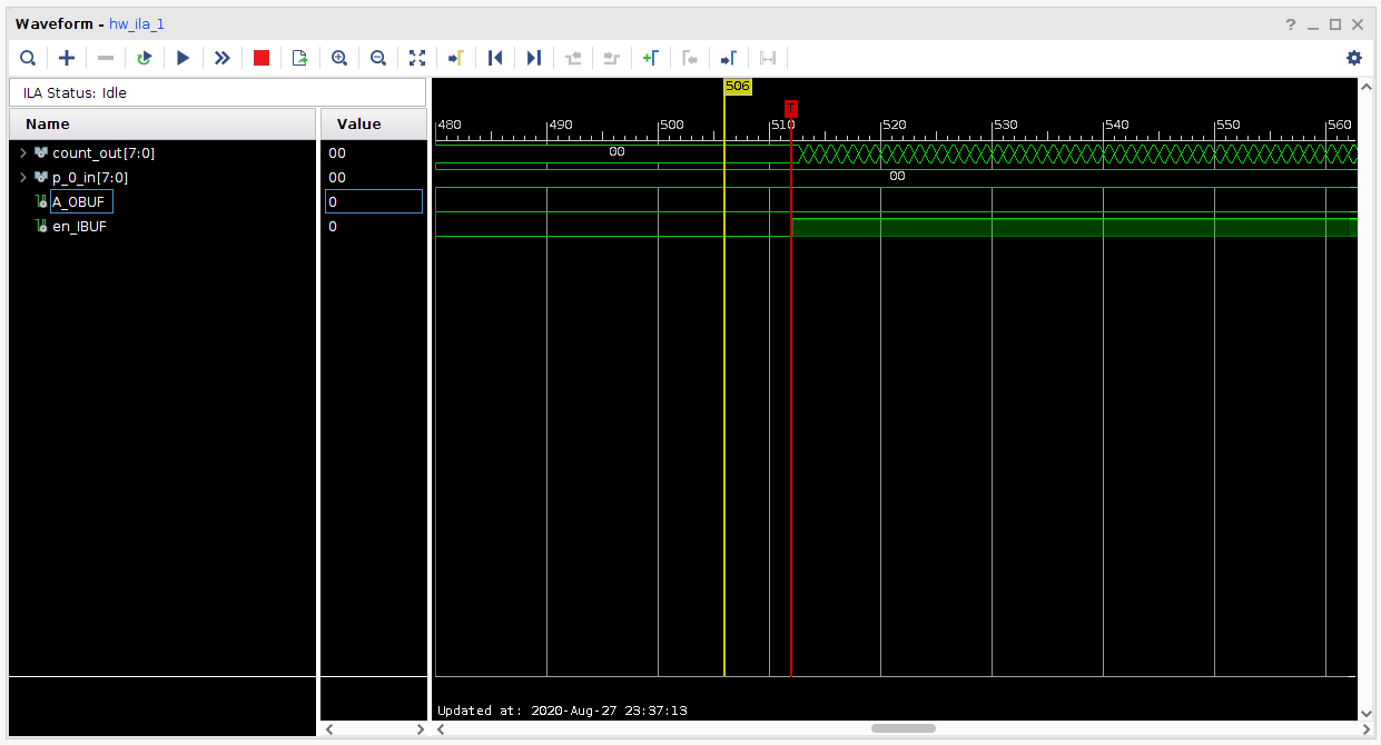
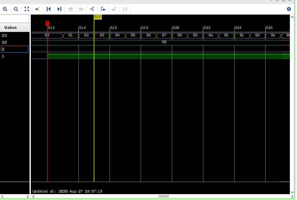
You can see in Figure 14 that the trigger time marker coincides with the transition in state (rising-edge) of the counter enable signal. The counter value also begins to change, though waveform is too zoomed-out to see the values of the counter. Using the zoom in/out buttons above the waveform display or the scrollwheel on a mouse, you can adjust the timescale of the waveform display.
Triggering using a integer value
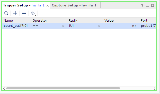
In addition to triggering based on the state of single wires, the value of busses may be used to trigger the ILA. This can be very useful when dealing with circuits that produce binary numbers, such as a counters or even computer data and address buses. In the example Trigger Setup Window shown below the ILA is set to trigger when the counter ouput value is equal to 67. Note that the Radix field is set to [U] for Unsigned Integer, This sets the base of the number entered in the value field.
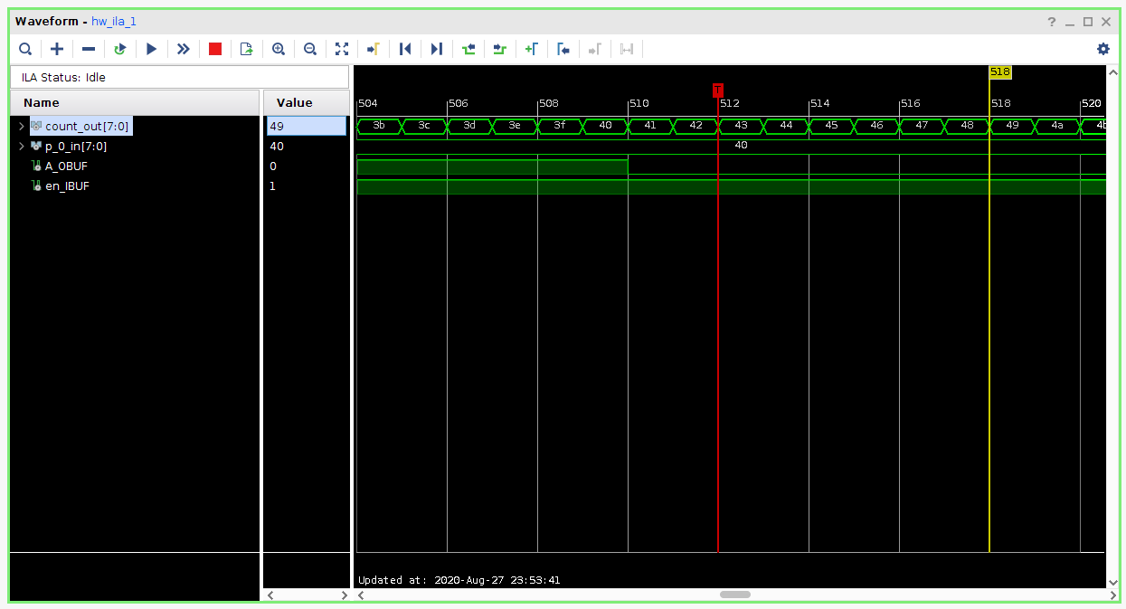
The figure below shows the result of the trigger; At count value 0x43 (decimal 67), the trigger occured, and data before and after the event was captured.
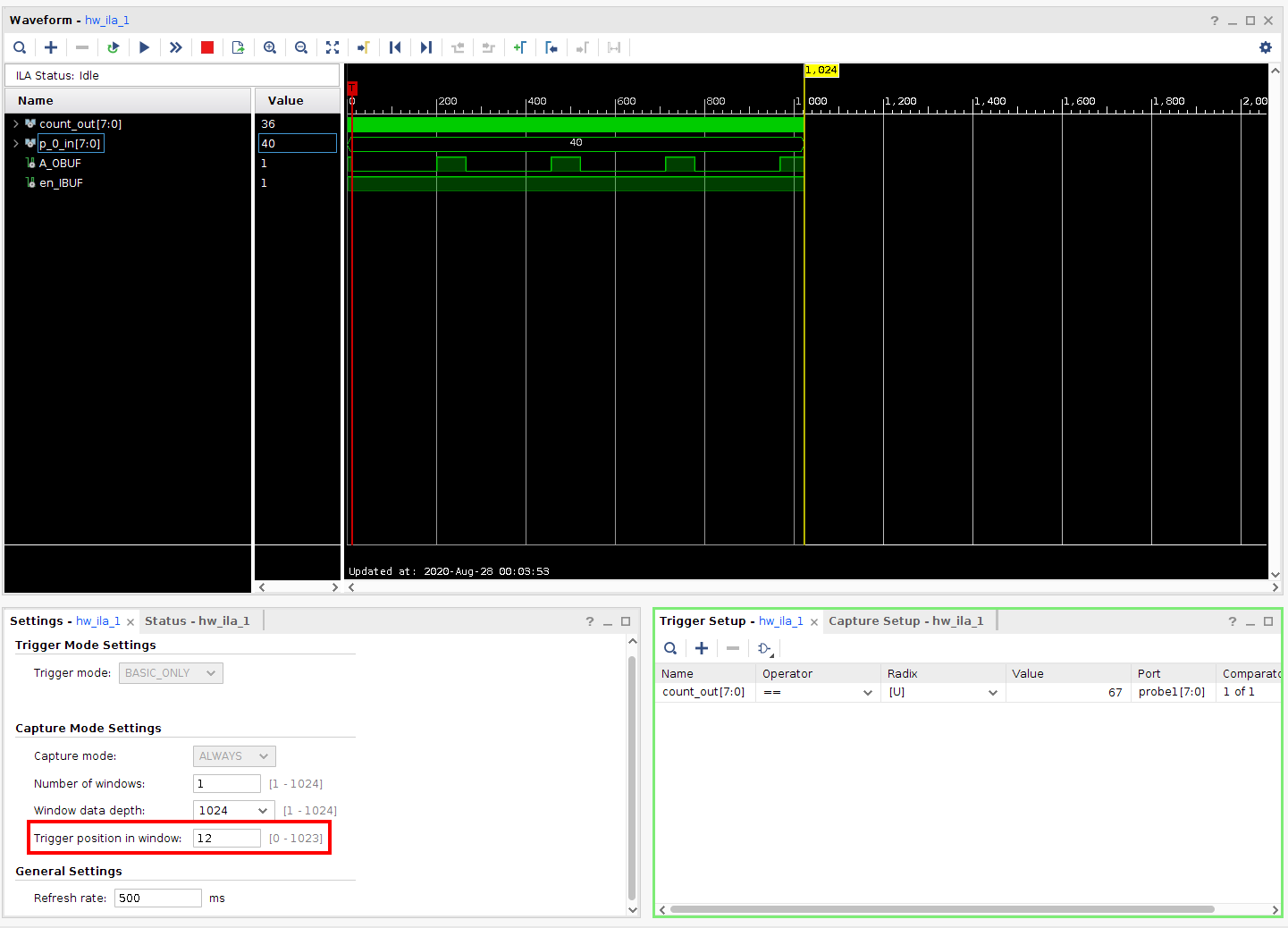
Setting the Trigger Position
All examples of ILA captures shown up to this point have been taken with an equal number of samples being captured before and after the trigger (the trigger is at sample 512 of 1024). In the Settings window this can be changed to set when the data is first collected and how long after the trigger data is collected. The window size (total number of samples) can also be changed here. The figure below shows a captured waveform with the window position set to 12 (this must be set prior to arming the trigger). At sample 12, there are 11 samples collected before the trigger occurs, and 1012 after the trigger.