Character ROM
Setting up Character ROM for VGA and HDMI

ASCII Code
ASCII is the acronym of American Standard Code for Information Interchange. It is an standard encoding used in computers to represent characters such as “a”, “A”, or “$”. ASCII code definition can be dated back to 1960s. In 1968, U.S. Department of Commerce published Code of Information Interchange, which defines a 7-bit encoding for the numbers 0-9, the letters a-z and A-Z, some basic punctuation symbols, and control codes originated from Teletype machines, and space. The ASCII table is shown as Figure 1.

Character ROM
A Character ROM is a device that converts ASCII code into a dot matrix pattern that can be displayed on screen. Figure 2 shows the character ‘0’ in 16 by 16 dot matrix. To save the storage of those dot matrix, one bit is used to mark whether a dot is marked or not in the dot matrix. So, the dot matrix of character ‘0’ can be represented using 16x16=256 bits (i.e. 32 Bytes). If each character in the ASCII table is represented using a 16 by 16 dot matrix, you will need a 256Bit—128Chars=32768Bits (it can be represented as 32KBits or 4KBytes) to store all those data.

Character ROM Implementation using Block RAM
In Xilinx FPGA, Block RAM is the built-in memory device that you can use to store those data. The block diagram of BRAM is shown in Figure 3. The description of each input and output ports are described in the table below.
| Signal | In/Out | Description |
|---|---|---|
CLK |
input | 1-bit input clock |
ADDR |
input | Input address, width defined by read/write port depth |
DO |
output | Output data, width defined by READ_WIDTH parameter |
DI |
input | Input data port, width defined by WRITE_WIDTH parameter |
WE |
input | Input write enable, width defined by write port depth |
EN |
input | 1-bit input RAM enable |
RST |
input | 1-bit input reset (active high) |
REGCE |
input | 1-bit input output register enable |
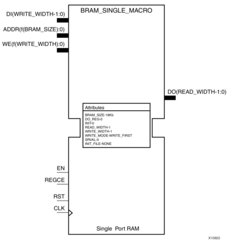
You can download the BRAM verilog file by clicking the button char_rom.v. Each character is encoded by 256 bits (16x16), i.e. 32 Bytes.
Width of Address and Data
In the file char_rom.v, a 36KBit Block RAM is instantiated using Verilog, initialized with 16 by 16 pixel matrix of all 128 ASCII character. As Block RAM built inside Xilinx FPGA allows user to add one parity bit for each byte, the BRAM size in the code is set to 36KBit instead of 32KBit as calculated in previous section. If the output data width is 8-bits, each address reads 1 byte of data from the BRAM. As a result, you need 12-bit address to cover all 4096 addresses of the Block RAM. In the char_rom.v the data output is 16 bits. Thus, you only need 10-bit address as there are only 2048 address to cover.
Behavioral of Block RAM
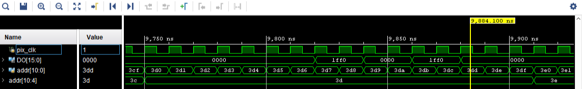
In order to know the behavioral of the block RAM, you can run a simulation on the char_rom.v. Keep in mind that the address of the charm ROM will need to be broken into two parts - [10:4] is the address of the character and [3:0] is the address of the line of the character. You should be able to see the characters drawn out in simulation if you used DO 16bit. Understanding how the char ROM works is crucial part of figuring out how to complete this project. Here is a sample test bench that you can run to simulate the behavioral of the BRAM.
`timescale 1ns / 1ps

module char_rom_tb(
    );

wire [15:0] DO;
reg pix_clk = 1'b1;
reg [10:0] addr = 11'd0;

// Generate pix_clk
always
begin
    #5 pix_clk <= ~pix_clk;
end

// Increment Address every clock cycle
always @ (posedge pix_clk)
begin
    addr <= addr + 1'b1;
end

char_rom char_rom_inst (
    .DO(DO),       // Output data, width defined by READ_WIDTH parameter
    .ADDR(addr),   // Input address, width defined by read/write port depth
    .CLK(pix_clk),     // 1-bit input clock
    .DI(16'h0),       // Input data port, width defined by WRITE_WIDTH parameter
    .EN(1'b1),       // 1-bit input RAM enable
    .REGCE(1'b0), // 1-bit input output register enable
    .RST(1'b0),     // 1-bit input reset
    .WE(2'd0)        // Input write enable, width defined by write port depth
    );
endmodule
The simulation of the block RAM is shown in the figure 4. Note that the data is valid on the data output signal DO on the rising edge of next clock cycle after the address is presented on the address input signal ADDR.
Block Diagram of VGA Controller with Char ROM

The block diagram of VGA controller with Character ROM is shown in Figure 5 above. Instead of displaying a constant color screen, the input I1 of the MUX that generates RGB is wired to another mux which decides which color (foreground color or background color) should be displayed at current pixel position (represented by h_count signal and v_count signal). To make that decision, with the assumption that the corresponding byte from character ROM has been available on the data output DO, you need to design some logic that find the corresponding bit in DO and generate the signal to control the MUX to select between foreground and background colors.
Now, another piece of logic needs to be designed to make sure that the corresponding byte from the character ROM is read in time when you need it to make the choice between foreground and background. So, the address generation logic will take in h_count, v_count, software defined locations of character (say loc_x and loc_y), and the ASCII code of the letter you want to display (ascii_code).
Simulate Before Implementation
As designs get more and more complicated, simulate your code before going straight into implementation. Moreover, you also need to pay attention to modularize your code. In this design, you have processors, DDR memory, AXI Interconnects, and VGA controller. Simulating the whole design will take a long long time. When you are creating modules, make sure to simulate existing modules before creating another one - take it one step at a time - this will save you a lot of time. Think about what should be your expected outcome after wrapping modules and check your thought process by simulating your wrapped modules.
The diagram that is provided in figure 5 is not the only way to do this project, for example, instead of using some shifting logic, you may use counters instead. You can assign constant input values for loc_x,loc_y, and ascii_code; then generate bitstream. This way you can save more time because you can validate whether or not your bitstream is working properly before jumping into Vivado SDK.
Here is a reference code for VGA controller simulation
`timescale 1ns / 1ps

module vga_core_tb(
    );

    reg reset_int = 1'b0;
    // RGB 8-8-8
    wire [23:0] background = 24'h00FF00;
    // Char ASCII
    wire [7:0] ascii_code = 8'h30; // '0'
    wire [23:0] foreground = 24'hFF0000;
    wire [12:0] char_x = 13'd192;
    wire [12:0] char_y = 13'd41;

    reg pix_clk = 1'b1;
    // Some other declarations
    ...

    // Generate Pixel Clock
    always
    begin
        #5 pix_clk <= ~pix_clk;
    end

    // Reset VGA controller at the beginning of simulation
    initial
    begin
        #10 reset_int = 1'b1;
        #20 reset_int = 1'b0;
    end

    // Instantiate your VGA Controller
    vga_core vga_core_inst (
        .reset_int(reset_int),
        .background(background),
        .ascii_code(ascii_code),
        .foreground(foreground),
        .char_x(char_x),
        .char_y(char_y),
        .pix_clk(pix_clk),
        // Other signal connections
        ...
    );
endmodule