Delay in Circuits
Introduction to delay and glitch

Step 1: Implement the Circuit in Verilog
In this project, you are going to implement a circuit in Verilog and simulate it, taking delay into consideration. The circuit schematic is shown in Fig. 1, and the delay of each gate is marked in red.

Declare the Combinational Circuit Module
The circuit shown in figure 1 has three inputs A, B, and C, and one output X. So, the declaration of the module goes as follows:
module CombCirc(
   input A,
   input B,
   input C,
   output X
   );

// Circuit Description

endmodule
Implement Circuit with Delay
The goal of this project is to simulate the delay of logic gates and analyze its effect on the circuit behavior. So, you need to describe each logic gate use an assign statement with delay command as shown in the code block below.
wire N1, N2, N3;

// AND gate with 1ns delay
assign #1 N1 = A & B;
// Not Gate with 1ns delay
assign #1 N2 = ~B;
// And Gate with 1ns delay
assign #1 N3 = N2 & C;
// Or Gate with 1ns delay
assign #1 X = N1 | N3;
In the codes above, N1, N2 and N3 are three internal signals as labeled in figure 1. Each gate has a delay of 1 reference time unit. In order to make the delay 1ns for each gate, you need to define the reference time unit as 1ns using command 'timescale at the beginning of the file.
`timescale 1ns / 1ps
module CombCirc(
...
Check Your Source File
So the Verilog file that describes the circuit with delay information of each gate looks as follows:
`timescale 1ns / 1ps
module CombCirc(
    input A,
    input B,
    input C,
    output X
    );

wire N1, N2, N3;

// AND gate with 1ns delay
assign #1 N1 = A & B;
// Not Gate with 1ns delay
assign #1 N2 = ~B;
// And Gate with 1ns delay
assign #1 N3 = N2 & C;
// Or Gate with 1ns delay
assign #1 X = N1 | N3;

endmodule
Step 2: Create the Test Bench and Simulate the Circuit
In order to simulate glitch, you will need to generate an input sequence in your testbench that can cause the glitch to appear at the output of the circuit. By observing the circuit, there is an unbalanced path between input B and output X (i.e., there are two paths to propagate the changes of B to the output with different delays). So, the glitch will happen when A and C are held constant and B is toggled. The codes below generates a sequence where B changes from 1 to 0 and back to 1 when A and C are held constant. Do not forget to instantiate the CombCirc module in your test bench and connect the inputs and outputs to internal signals!
integer k = 0;

initial begin
    // Initialize Inputs
    A = 0;
    B = 0;
    C = 0;

    // Wait 100 ns for global reset to finish
    // Add stimulus here

    for(k = 0; k < 4; k=k+1)
    begin
        {A,C} = k;
        #5 B = 1;
        #5 B = 0;
        #5 ;
    end
end
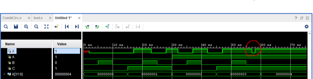
Simulate the test bench
Now, you can simulate your test bench in the Vivado simulator, and you will get the waveform as shown in figure 2 below. The red circle on the waveform specifies the glitch. It happens when A is 1, C is 1 and B changes from 1 to 0. The duration of the glitch is 1ns.