UART and GPIO Controller
Configuring the PS MIO connections in vivado and using a AXI GPIO Controller IP Core

Introduction
For Project 5, you will need some form of input to manipulate the character displayed on the screen as well as it’s parameters (location, color, etc). This pre-lab is intended to (re)familiarize you with the Zynq’s UART module. It will also cover an easy method of reading switch and button values from a c program.
Background
MIO System
The Processing System portion of the Zynq SoC contains 2 UART modules. Using these, the processor can communicate in standard serial protocol with PC’s and other devices. The signals of processing system hard-silicon peripherals can be accessed in the FPGA, but they are also accessible on dedicated Pins on the Zynq SoC’s package. On the blackboard one RGB-LED is connected to three MIO pins, as well as 2 additional pushbuttons (on the board you can see there is an indicator for MIO 50 and 51 below these buttons). If you looked into the blackboard’s schematic you would see there are indeed 2 push buttons connected to MIO pins 50 and 51. Some other devices on the blackboard are connected to MIO pins as well; The bluetooth radio is connected to MIO through both its SPI and UART interfaces, the I2C bus of the NXP temperature sensor is connected via MIO as well. To make a system designer’s task easier, MIO can be mapped to specific functions (though some pins may only connect to a subset of the peripheral I/O available). In some cases a pin might need to be a simple digital output (driving an LED, for example) in others it might need to be configured as the receiver input for a serial bus. Both FPGA and MIO pins are reconfigurable, however FPGA pins are typically only configured at FPGA-program time, where MIO pins can be configured both at boot-time and in the middle of a program. This project will cover configuring your zynq block design so it boots up with the MIO pins connected to an FTDI UART-USB bridge already configured for UART operation.
Requirements
1. Configure the ZYNQ MIO pins to connect UART1 to the FTDI UART-USB Bridge
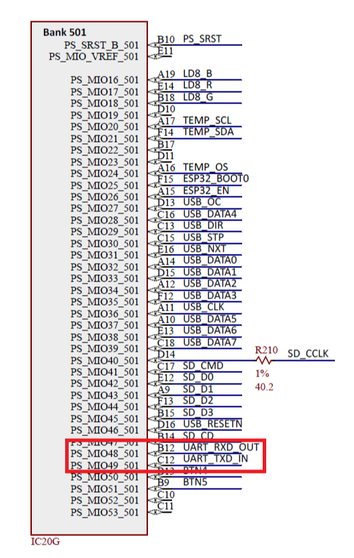
Before you can configure UART 1 to communicate to the PC from the blackboard, you need to configure the MIO system to connect to UART transmit (TX) and receive (RX) pins to the corresponding RX and TX on the UART-USB bridge. In the schematic (seen in figure 1), you can see MIO pins 48 and 49 are connected to the FTDI USB-UART bridge.
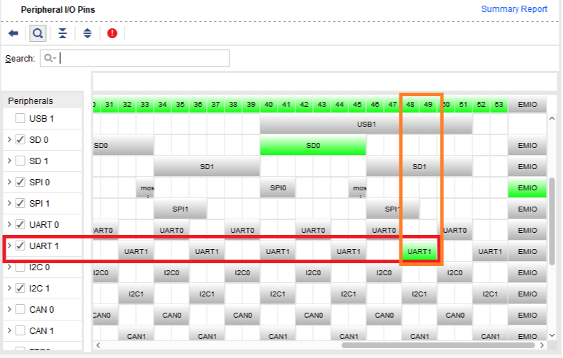
To configure pins 48 and 49 to connect to the UART module at boot time, you can configure the zynq block in vivado’s block design tool. Refer to figure 2, in the Peripheral I/O Pins tab, you can enable MIO pins 48 and 49 for UART 1, then at boot-up the zynq will mux the rx/tx pins of the UART1 module to the selected pins; By configuring them in the block design your program will not need to initialize the MIO pins in software before configuring the UART module.
To complete the requirement your block will also need an instance of your LED controller from project 2. This will be used to display outputs from characters received over UART.
Implement your system and write a C program which does the following: In a loop, receive characters over UART, send back (echo) any characters received to the terminal, then display the value of the last received character as binary on the board’s LEDs. Do not change the LED value for newline characters as they will be the last character sent from the vitis terminal, if you do not ignore newlines or carriage returns, you may never see the value change, regardless of what characters you send.
Your terminal should show the same text you sent to the board and the LEDs should display the binary value of the last ascii character received. For example, if the last character received was lowercase ‘k’, the ascii value would be hexadecimal ‘0x6B’, or binary ‘0b01101011’.
Refer to the background documents on how to configure and use the Zynq’s built-in UART controllers. For this lab a driver is provided in the header/source pair below
#ifndef UART_H
#define UART_H

#include <stdint.h>

//memory mapped register base address and offsets
#define UART1_BASE		0xE0001000

#define UART1_CR		(*(uint32_t *)(UART1_BASE))
#define UART1_MR		(*(uint32_t *)(UART1_BASE+4))
#define UART1_SR		(*(uint32_t *)(UART1_BASE+0x2C))
#define UART1_DATA		(*(uint32_t *)(UART1_BASE+0x30))
#define UART1_BAUDGEN	(*(uint32_t *)(UART1_BASE+0x18))
#define UART1_BAUDDIV	(*(uint32_t *)(UART1_BASE+0x34))


//macros for checking bits in the SR

//1 if uart1 tx is not full, 0 if full
#define UART1_TX_READY()	((UART1_SR&0x10)==0)
//1 if uart1 rx has data, 0 if empty
#define UART1_RX_READY()	((UART1_SR&2)==0)

//constants for generating a standard baud rate
#define BGEN_115200 0x7C
#define BDIV_115200 6


//init configure functions
void init_uart1(void);
void set_baud_uart1(uint32_t bgen, uint32_t bdiv);
void conf_uart1_115200(void);

//character tx/rx functions
void putc_uart1(char val);
char getc_uart1(void);

//string print function
void putst_uart1(char *str);

#endif
#include "uart.h"

//configures the uart to talk to the FTDI USB on the blackboard
void conf_uart1_115200(void)
{
	init_uart1();
	set_baud_uart1(BGEN_115200,BDIV_115200);
}

//resets and configures uart module for 8 data bits, 1 stop bit, no parity
void init_uart1(void)
{

	//reset uart module
	UART1_CR = 3;

	//wait for reset to clear
	while(UART1_CR&0x3);

	//configure UART mode register
	//normal mode   [9:8] = 2b00
	//one stop bit  [7:6] = 2b00
	//no parity     [5:3] = 3b1xx
	//8 data bits   [2:1] = 2b0x
	//use ref clock [0:0] = 1b0

	//bin10b 00 001x x0x0
	//hex10x 0  2    0
	UART1_MR = 0x20;

	//configure UART control register
	//bit2=1, enable tx
	//bit4=1, enable rx
	UART1_CR = 4 | 16;
}


//set the values for the bgen and bdiv registers
void set_baud_uart1(uint32_t bgen, uint32_t bdiv)
{
	UART1_BAUDGEN=bgen;
	UART1_BAUDDIV=bdiv;
}

//waits until there is room in tx fifo and then enqueues 'val'
void putc_uart1(char val)
{
	//wait for room in output fifo
	while(!UART1_TX_READY());

	//now there is room, we can queue up the data
	UART1_DATA = val;
}

//waits until a character is available from rx fifo then dequeues and returns character value
char getc_uart1(void)
{
	uint32_t val;

	//wait for a character to arrive
	while( !UART1_RX_READY() );

	//copy from fifo
	val = UART1_DATA;

	//return lower 8 bits
	return val&0xFF;
}

//prints null terminated string "str" out on uart1
//string MUST have a null terminating character
void putst_uart1(char *str)
{
	int i;
	i=0;
	while(str[i]!='\0')
	{
		putc_uart1(str[i]);
		i+=1;
	}

}
2. Configure an AXI GPIO controller to read Switch and Button Values
In order to read switch and button values in a c program, the input pin values will need to be sent over the AXI bus to the processor. You could create your own AXI logic to do this, however Xilinx provides an easy to use IP Core that can perform this function. For this lab you are expected to use the AXI GPIO controller, but if you implemented your own switch-reading IP you are welcome to use it.
Adding and configuring the AXI GPIO Controller in Vivado block design
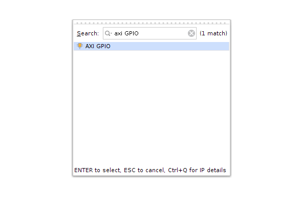
Search for the AXI GPIO IP core in the IP catalog and add it to your block design:
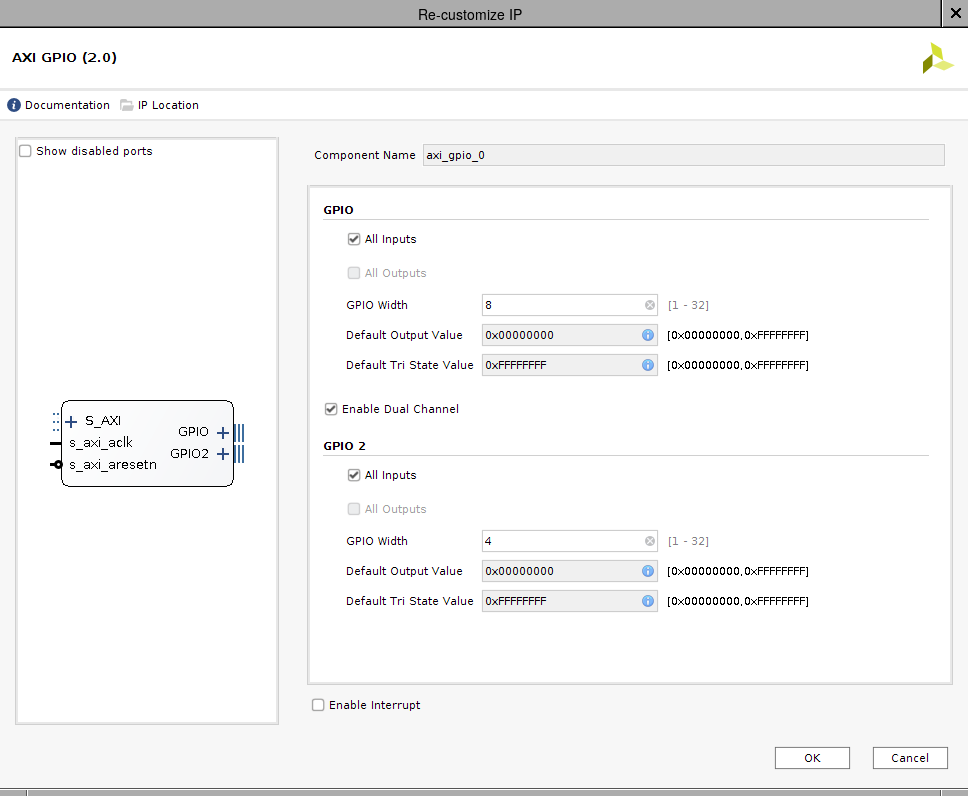
Configure the IP Core for dual channel operation, inputs only. Configure one channel to be 8-bits wide and the other to be 4-bits wide. The example dialogue in figure 4 is configured as described.
Hook up the output of the first 8 slide switches to the 8-bit wide input and the output of the 4 pushbuttons to the 4-bit wide input. When Finished your module should appear the same as in figure 5.
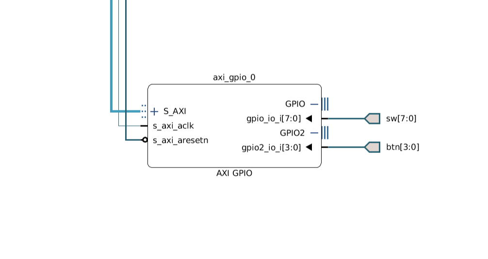
Make note of the base address of the module so you can write a driver in c to read values from your switches and buttons.
Write a function for reading the current switch value from the GPIO IP core, and another function for reading the current button values. Prototypes for these functions are provided below.
//Reads switch value from the GPIO module and returns in bottom 8-bits of a 32 bit integer
uint32_t read_sw_val(void);

//Reads button value from the GPIO module and returns in bottom 4-bits of a 32 bit integer
uint32_t read_btn_val(void);
The AXI GPIO Controller IP Core’s register definition is shown below. This register definition is only valid when the module is configured for ‘read-only’ mode. Consult the IP’s documentation from xilinx for further usage information (including use in GPIO mode).
| Address | Reg Name | Valid Bits | Reset Value | Description |
|---|---|---|---|---|
| BASE_ADDR+0x0 | GPIO1_DATA | [WIDTH-1:0] | 0 | Read data for this GPIO port. Reading returns value input into the module. |
| BASE_ADDR+0x4 | GPIO1_TRI | [WIDTH-1:0] | 0 | Tristate value for this GPIO port. Always read as 0, writes have no effect. |
| BASE_ADDR+0x8 | GPIO2_DATA | [WIDTH-1:0] | 0 | Read data for this GPIO port. Reading retunrs value input into the module. |
| BASE_ADDR+0xC | GPIO2_TRI | [WIDTH-1:0] | 0 | Tristate value for this GPIO port. Always read as 0, writes have no effect. |
Write a program that periodically prints the value of the switches and the buttons out to the terminal. Format the values as Hex integers. An example of what your output might be like is shown below (Note as the buttons are a 4-bit input, the upper hex digit should always be zero)
SW Val: 0x34
BT Val: 0x02

SW Val: 0xFA
BT Val: 0x08
You can use the code below to get started
//prototype for function called in main
void byte_to_hex_str(uint8_t val, char *str);


int main(void)
{

	//buffer for holding output string
	char disp_str[8];


	//configure uart1 to talk to the ftdi module properly
	conf_uart1_115200();

	//variable for holding values read from switches
	uint32_t read_val;

	//indicate start of program
	putst_uart1("******************************************\n\r");
	putst_uart1("READY!\n\r");

	for(;;)
	{

		//read value from switches
		read_val =

		//create output string from read value
		byte_to_hex_str( (read_val&0xFF), disp_str);

		//print value string and formatting text

		//repeat the above but for displaying button values


		//delay for a noticeable amount of time

	}

	return 1;
}

//returns the ascii character of the value of the lower 4 bytes in 'val'
char nibble_to_hex(uint8_t val)
{
	val &= 0xF;

	//if value is A-F, add offset of 'A' character
	//else add offset of '0' character
	val += (val>9)? + ('A'-10) : '0';

	return val;
}

//creates a null terminated string from the value of an 8-bit integer
//string is always 3 characters: 2 hex digits and terminating character.
void byte_to_hex_str(uint8_t val, char *str)
{

	//convert upper nibble to hex character
	str[0] = nibble_to_hex( (val>>4)&0xF );

	//convert lower nibble to hex character
	str[1] = nibble_to_hex( val&0xF );

	//terminate string
	str[2] = '\0';
}