AXI4-Lite Interface
Introduction to AXI4-Lite

Introduction to AXI4-Lite (Advanced Extensible Interface)
Advanced eXtensible Interface 4 (AXI4) is a family of buses defined as part of the fourth generation of the ARM Advanced Microcontroler Bus Architectrue (AMBA) standard. AXI was first introduced with the third generation of AMBA, as AXI3, in 1996.
The AMBA specification defines 3 AXI4 protocols:
- AXI4: A high performance memory mapped data and address interface. Capable of Burst access to memory mapped devices.
- AXI4-Lite: A subset of AXI, lacking burst access capability. Has a simpler interface than the full AXI4 interface.
- AXI4-Stream: A fast unidirectional protocol for transfering data from master to slave.
Use in Xilinx-Based designs
Xilinx Vivado helps in the creation of custom IP with AXI4 interfaces. These can be connected to the Zynq’s Proccessing System or to other devices. This Document will cover the operation of the AXI4-Lite interface, which is convenient for implementing memory mapped registers.
AXI4-Lite Interface Signals
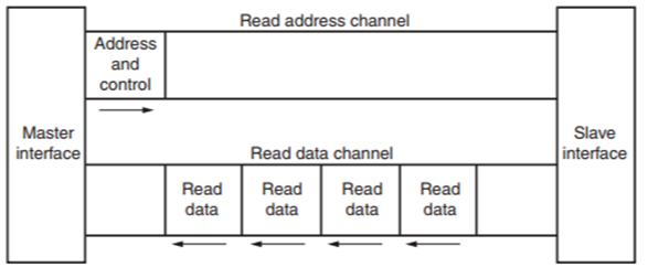
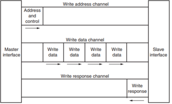
The AXI4-Lite interface consists of five channels: Read Address, Read Data, Write Address, Write Data, and Write Response. An AXI4 read transaction using the Read Address and Data channels is shown in figure 1. Similarly an AXI4 write transaction using the Write Address, Data, and Response channels is shown in figure 2. Note that these figures depict burst transfers, which AXI4-Lite is incapable of.
The following table provides a detailed explanation about each signals on AXI4-Lite Interface.
| Global Signals | ||
|---|---|---|
ACLK |
Clock source. | |
ARESETN |
Global reset source, active low. | |
| Read Address Channel | ||
|---|---|---|
| Name | Direction | Descrption |
ARADDR |
Read address, usually 32-bit wide. | |
ARCACHE |
Memory type. Xilinx IP usually ignores this value if a slave. IP as a master generates transactions with Normal Non-cacheable Modifiable and Bufferable (0011). | |
ARPROT |
Protection type. Xilinx IP usually ignores as a slave. As a master IP generates transactions with Normal, Secure, and Data attributes (000). | |
ARVALID |
Read address valid. Master generates this signal when Read Address and the control signals are valid. | |
ARREADY |
Read address ready. Slave generates this signal when it can accept the read address and control signals. | |
| Read Data Channel | ||
|---|---|---|
| Name | Direction | Descrption |
RDATA |
Read Data (32-bit only). | |
RRESP |
Read response. This signal indicates the status of data transfer. | |
RVALID |
Read valid. Slave generates this signal when Read Data is valid | |
RREADY |
Read ready. Master generates this signal when it can accept the Read Data and response. | |
| Write Address Channel | ||
|---|---|---|
| Name | Direction | Descrption |
AWADDR |
Write address, usually 32-bits wide. | |
AWCACHE |
Memory type. Slave IP usually ignores and Master IP generates transactions as Normal Non-cacheable Modifiable and Bufferable (0011). | |
AWPROT |
Protection type. Slave IP usually ignores and Master IP generates transactions with Normal, Secure and Data attributes (000). | |
AWVALID |
Write address valid. Master generates this signal when Write Address and control signals are valid | |
AWREADY |
Write address ready. Slave generates this signal when it can accept Write Address and control signals | |
| Write Data Channel | ||
|---|---|---|
| Name | Direction | Descrption |
WDATA |
Write data (32-bit only). | |
WSTRB |
Write strobes. 4-bit signal indicating which of the 4-bytes of Write Data. Slaves can choose assume all bytes are valid | |
| Write Response Channel | ||
|---|---|---|
| Name | Direction | Descrption |
BRESP |
Write response. This signal indicates the status of the write transaction. | |
BVALID |
Write response valid. Slave generates this signal when the write response on the bus is valid. | |
BREADY |
Response ready. Master generates this signal when it can accept a write response | |
Clock and Reset
Any AXI component has two global signals: the clock ACLK and an active-low asynchronous reset ARESETN. All AXI4 signals are sampled on the rising edge of the clock and all signal changes must occur aftert the rising edge.
Handshake Process
All five transaction channels use the same VALID/READY handshake process to transfer address, data, and control information. This two-way flow control machanism means both the master and slave can control the rate at which the information moves between master and slave. The information source generates the VALID signal to indicate when the address, data or control information is available. The information destination generates the READY signal to indicate that it can accept the information. The handshake completes if both VALID and READY signals in a channel are asserted during a rising clock edge.
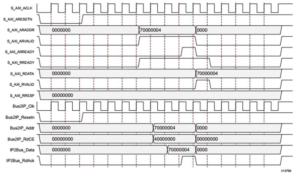
AXI4-Lite Read Transaction
Below, the sequence for an AXI4-Lite read is shown:
A description of the events in figure 3 follows:
- The Master puts an address on the Read Address channel as well as asserting ARVALID,indicating the address is valid, and RREADY, indicating the master is ready to receive data from the slave.
- The Slave asserts ARREADY, indicating that it is ready to receive the address on the bus.
- Since both ARVALID and ARREADY are asserted, on the next rising clock edge the handshake occurs, after this the master and slave deassert ARVALID and the ARREADY, respectively. (At this point, the slave has received the requested address).
- The Slave puts the requested data on the Read Data channel and asserts RVALID, indicating the data in the channel is valid. The slave can also put a response on RRESP, though this does not occur here.
- Since both RREADY and RVALID are asserted, the next rising clock edge completes the transaction. RREADY and RVALID can now be deasserted.
AXI4-Lite Write Transaction
Below, the sequence for an AXI4-Lite write is shown:
A description of the events in figure 4 follows:
- The Master puts an address on the Write Address channel and data on the Write data channel. At the same time it asserts AWVALID and WVALID indicating the address and data on the respective channels is valid. BREADY is also asserted by the Master, indicating it is ready to receive a response.
- The Slave asserts AWREADY and WREADY on the Write Address and Write Data channels, respectively.
- Since Valid and Ready signals are present on both the Write Address and Write Data channels, the handshakes on those channels occur and the associated Valid and Ready signals can be deasserted. (After both handshakes occur, the slave has the write address and data)
- The Slave asserts BVALID, indicating there is a valid reponse on the Write response channel. (in this case the response is 2’b00, that being ‘OKAY’).
- The next rising clock edge completes the transaction, with both the Ready and Valid signals on the write response channel high.
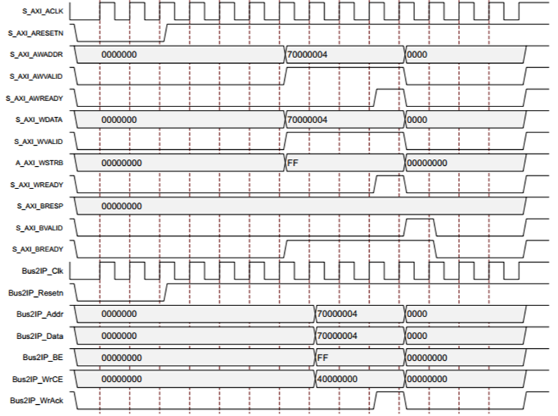
Note: The Handshakes on the Write Address and Write Data channel do not neccessarily occur simultaneously (as they do in the shown transaction). However, the AXI4 specification states that both must occur before the slave can send a write reponse. Both Write Address and Write Data handshakes can occur independently or simultaneously and no order is enforced, only that both must occur to complete the transaction.