Preparing a hardware design for ZYNQ
Create a ZYNQ hardware project with custom IP

Introduction
This tutorial demonstrates how to construct a simple digital system by adding a custom IP block to the ARM processor. There are quite a few steps, but once you go through the process and begin to understand what’s happening in each step, the process seems more straightforward. Steps include creating a top-level block diagram that includes a processor block and a custom IP block, properly configuring the IP block on the AXI bus, defining the IP block’s function in Verilog, generating an HDL wrapper, defining external pin connections, and programming the Blackboard. Once the hardware system has been defined, you can use the SDK tool to write code for your system.
Create a Block Design
This project uses the Xilinx IP integrator tool to create a system block diagram. This tool allows you to instantiate the ARM core, and add various peripherals. In this case, we will define a new AXI peripheral IP block to control the LEDs - the Verilog behavior (inside the IP block) is defined in a later step. Note the block diagram is drawn automatically, and may not have the appearance you desire (you can move the blocks around).
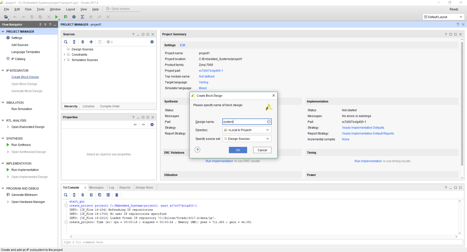
To create a block design, click on the Create Block Design under heading IP Integrator within Flow Navigator panel on the left. A Create Block Design dialog window will appear, and type system as the name of the design.
Create and Configure PS System
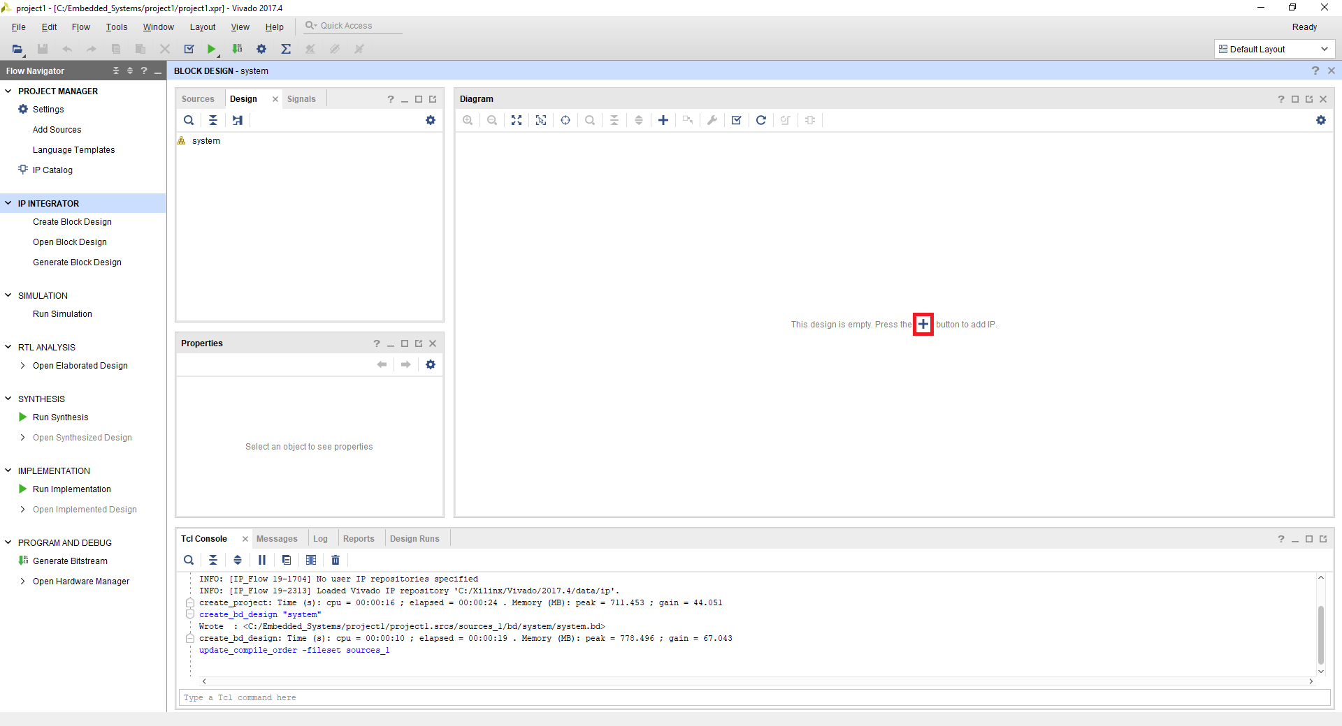
After the system block design is created, it is opened automatically. On the top right of Block Design window, there is a Diagram panel. Press the Add IP icon  to insert Zynq7 Processing System IP.
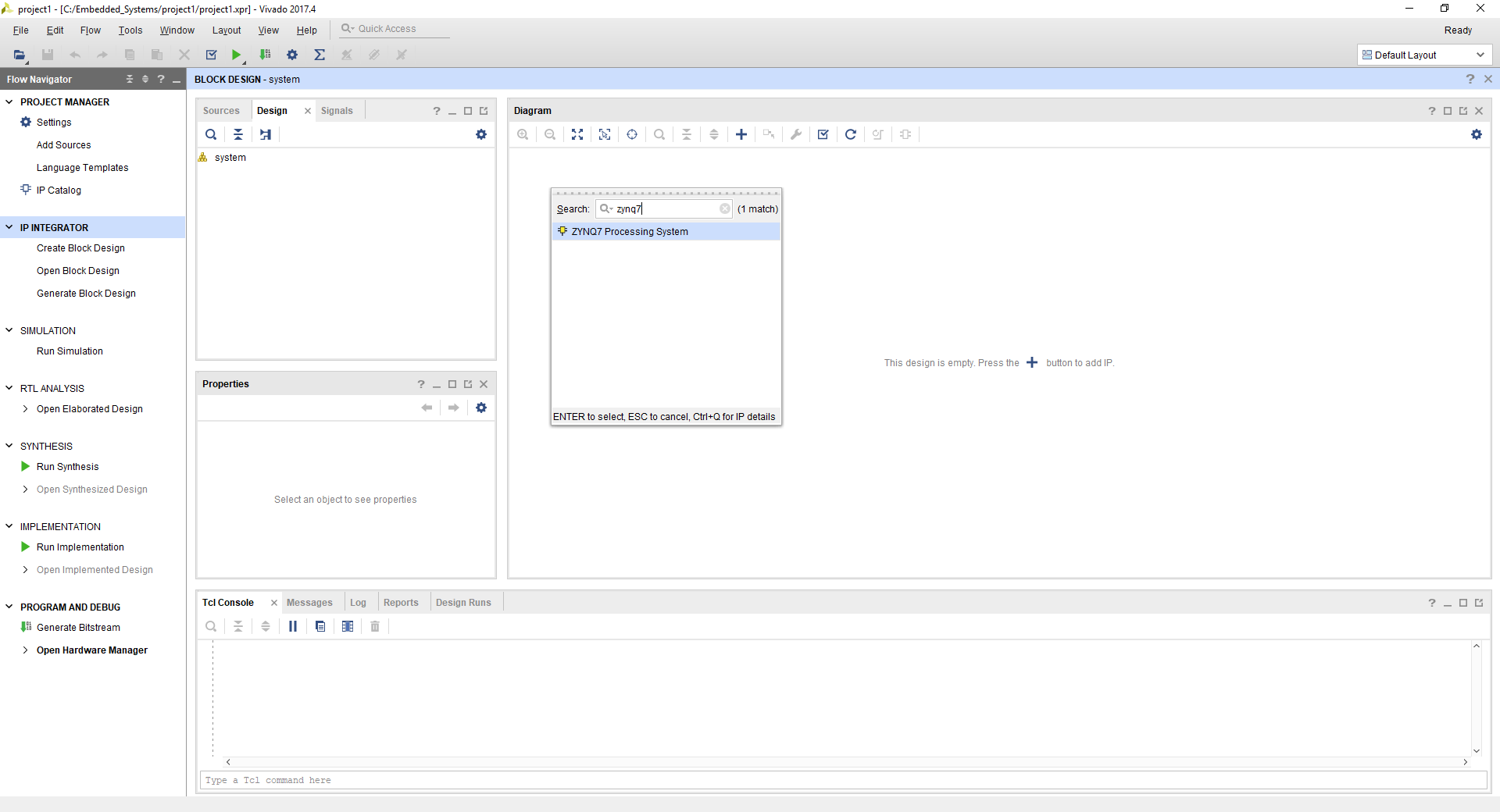
In the pop-up list, type Zynq into the search box and you will find IP Zynq7 Processing System as shown in Figure 3. Press Enter or double click it to add the IP into your block diagram.
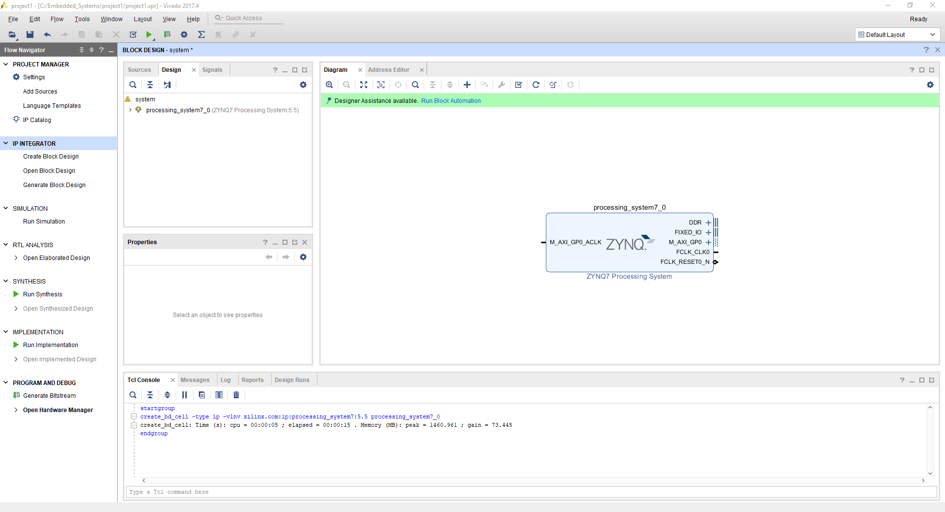
After you add the ZYNQ7 Processing System IP into the block design, the ZYNQ7 Processing System block will show up in the diagram panel with its inputs and outputs labeled and the block is named as processing_system7_0. The processing_system7_0 will also show up in the Design panel located at the top left corner of Block Design window.
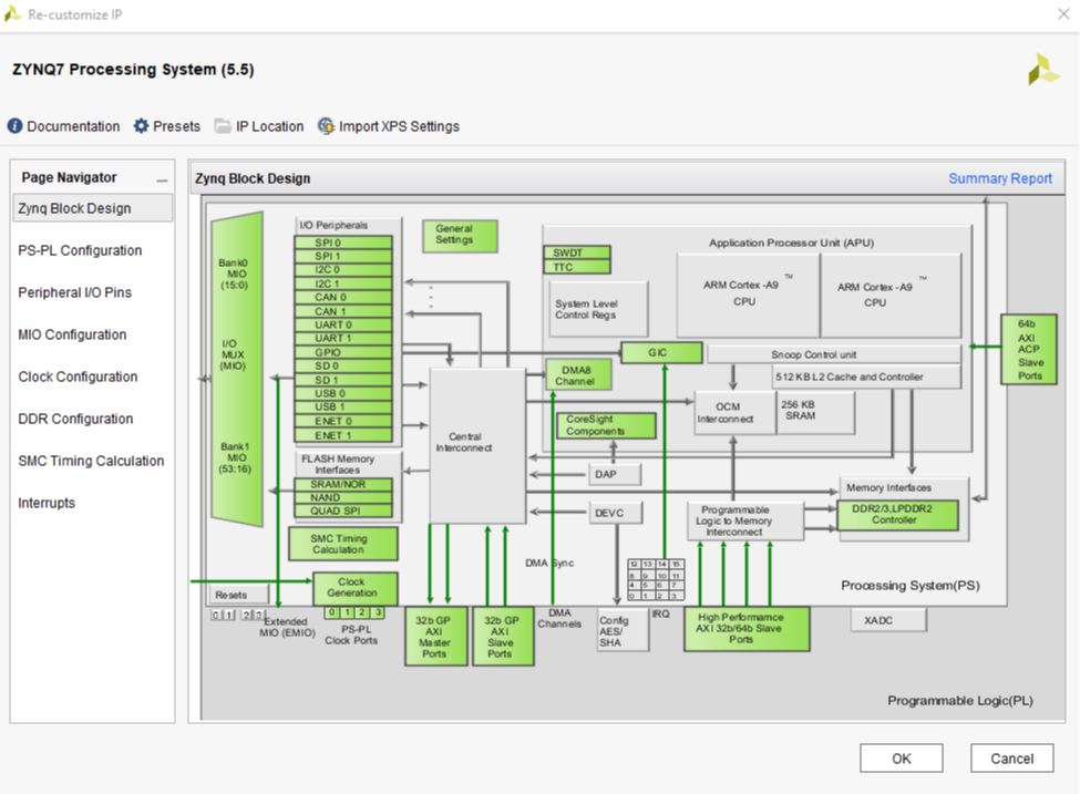
Double click ZYNQ7 Processing System block to bring up the configuration dialog.
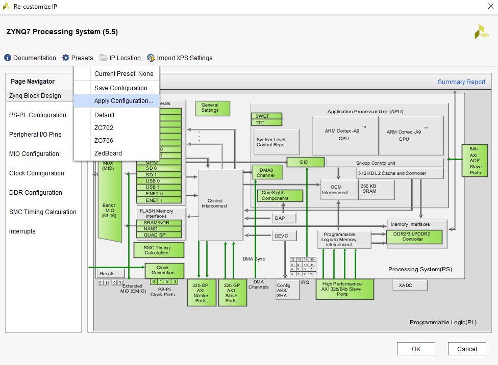
You can download the preset configuration of the processing system IP core for Blackboard using the button: Blackboard PS Preset
Click Presets, select Apply Configuration… and browse to blackboard_ps_preset.tcl file available from the button above to load the preset configuration of the PS system for Blackboard.
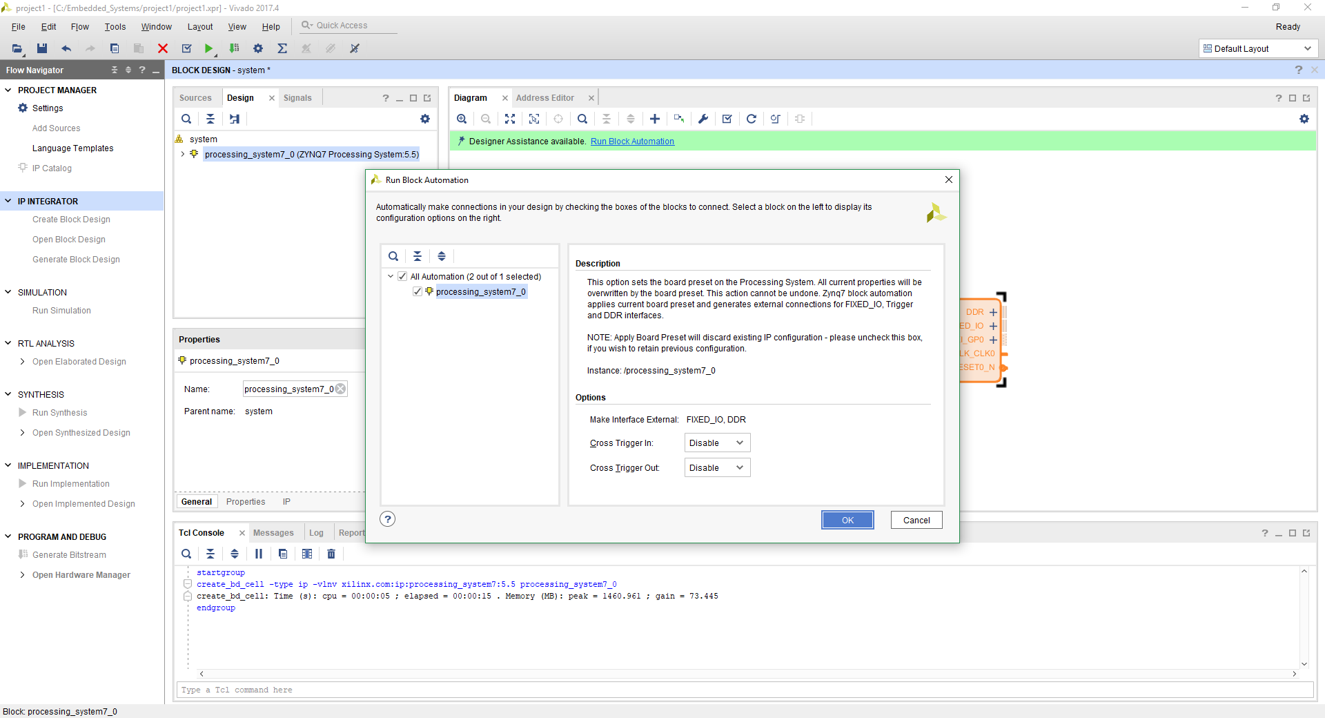
Click OK to finish configuring ZYNQ7 Processing System, and then click Run Block Automation to bring up Run Block Automation Dialog. In the dialog, keep everything as default and click OK.
Create LED Controller IP
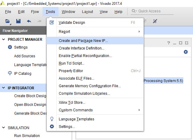
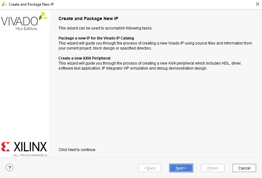
Now it is the time to create our own LED controller IP to the system. Open Tools menu and click Create and Package IP…
The Create and Package IP dialog will appear. click Next.
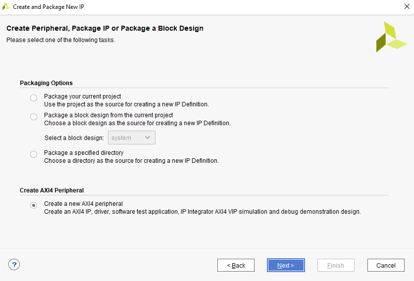
Select Create a new AXI4 Peripheral as shown in Figure 10. With AXI4 system bus attached, the LED controller will be mapped into the memory space of the ARM processor in PS, so that we can write software to control the status of on-board LEDs.
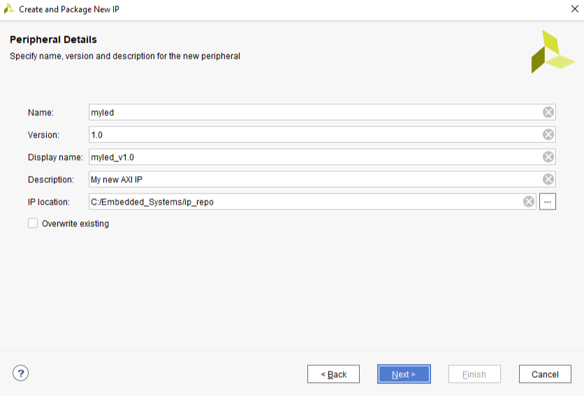
Put in the name of the IP, version, display name, and description into the dialog. Pick a place for IP location so that you can re-use your IP later on. After the creation, you will find your IP in the IP catalog of your project as well. Click Next when you are done.
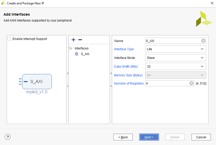
Now, you need to configure the AXI interface. ARM processor uses AXI (stands for Advanced eXtensible Interface) protocol to load and store data from peripheral controllers. As shown in Figure 12, we will name our AXI interface S_AXI, and choose Lite as interface type. The data width of the interface is 32-bit. As there are only 4 on-board Non-RGB LEDs, you only need 4-bit to be accessible to the CPU. But because Vivado requires a minimum of 4 registers, we will instantiate 4 registers in this controller. If you need more register, you may modify the code itself in the future for this specific IP, or you can create another IP with more registers.
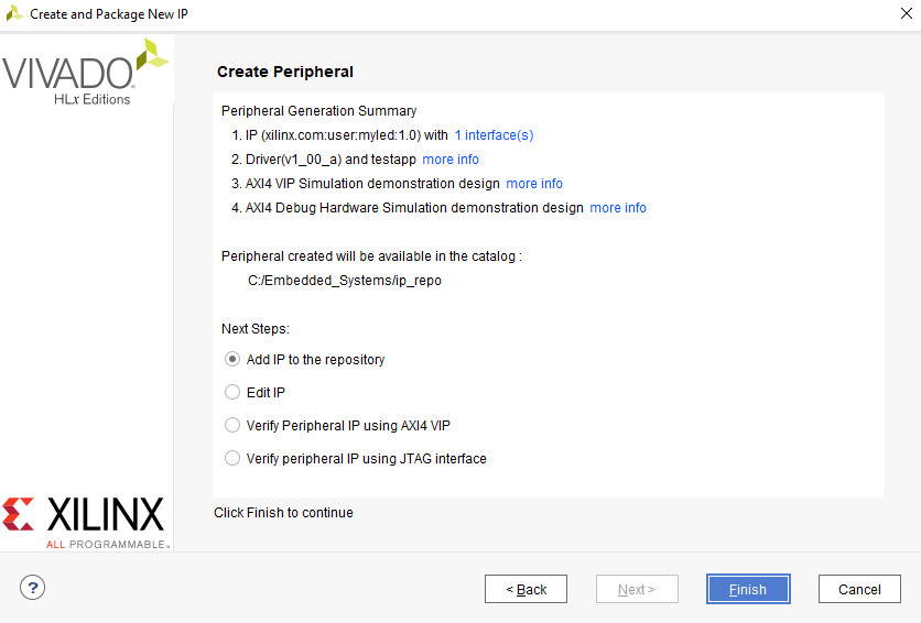
On the last page of Create or Package IP dialog, it will show a summary of the IP you just generated. Select Add IP to Repository and click Finish to finish create this IP.
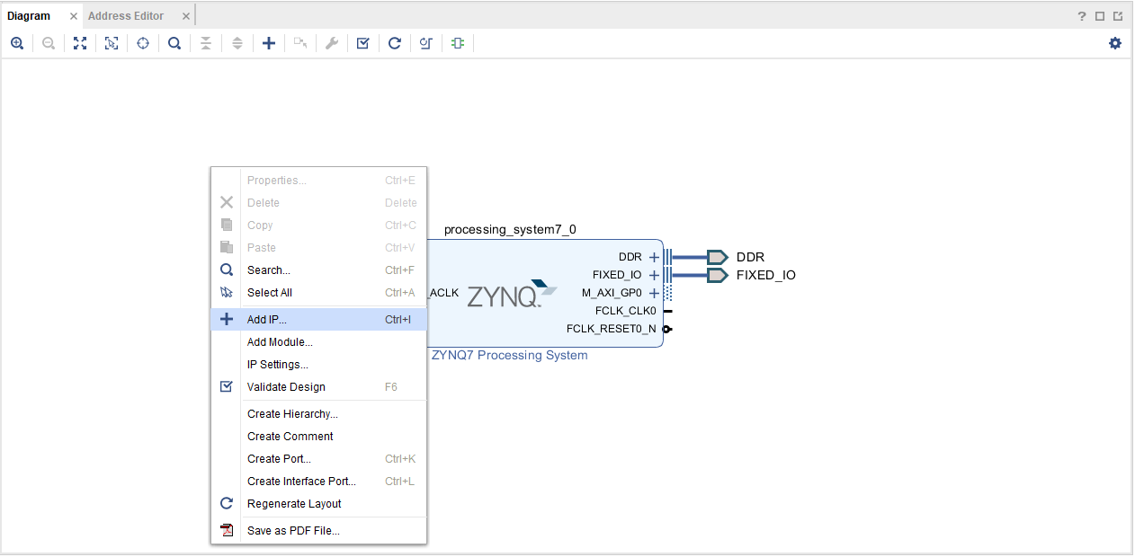
To add your newly created myled IP to your block diagram, find an empty space, right click and select Add IP.
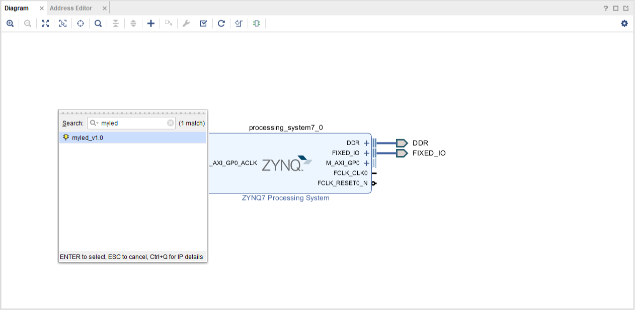
Type myled in search box and double click on myled_v1_0 to add myled IP into the diagram.
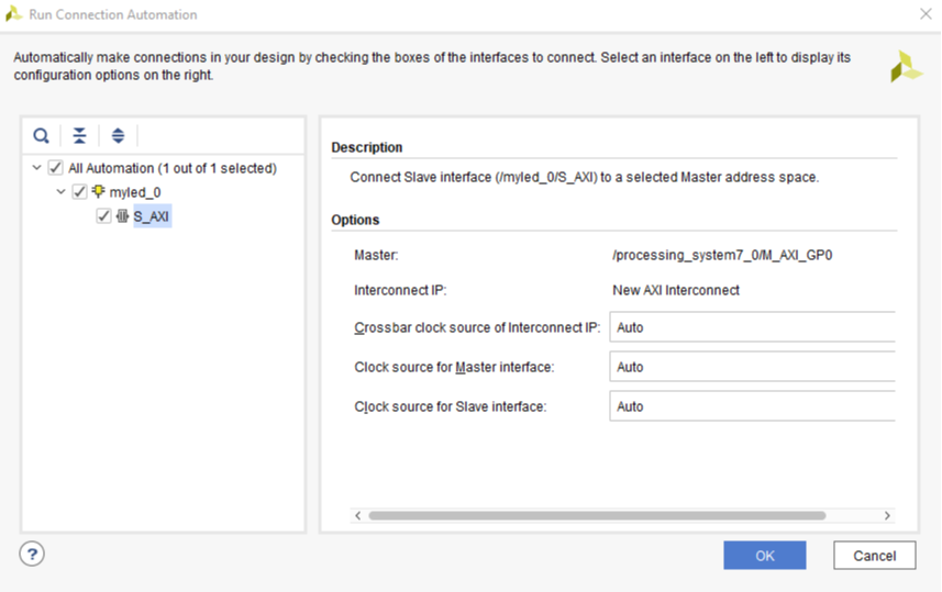
Click Run Connection Automation and bring up the Run Connection Automation dialog.
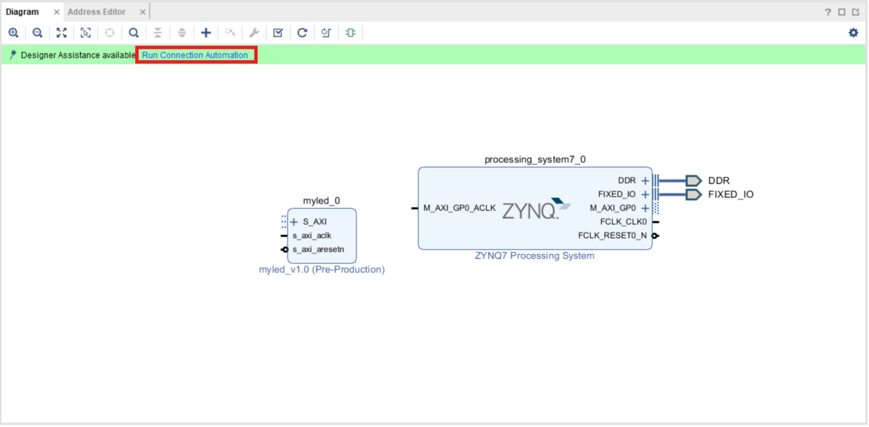
Select S_AXI interface of myled_0 IP on the left. Check the Master on the right is set to /processing_system7_0/M_AXI_GP0. Leave the Clock Connection to Auto. Click OK to let Vivado make the connection for you.
Check AXI Connection and Memory Map of LED Controller
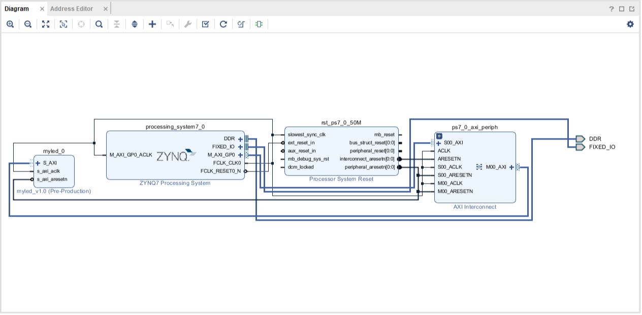
After the connection automation, Vivado will add a Processing System Reset IP Core to manage all the reset signals in the system, and an AXI Interconnect IP Core to connect peripheral controllers with AXI interface in the peripheral logic (PL), and map registers of those peripheral controllers into the ARM processor memory space. You can press Regenerate Layout Icon  redraw the block diagram.
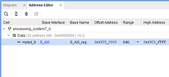
Click Address Editor to see the memory address mapping of myled_0 controller. As shown in Figure 19, the myled_0 controller is intially mapped from address 0x43C00000 to 0x43C0FFFF.
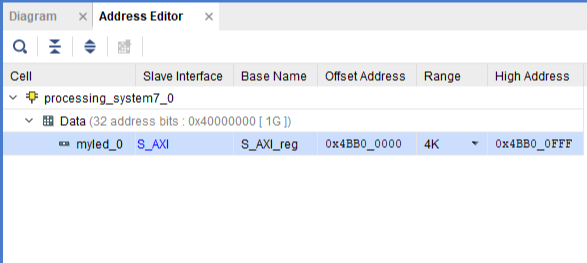
Since you won’t be using this much of memory space, modify the address editor as shown in figure 20 so that the range would be 4K and offset address would be 0x4BB0_0000. Notice that myled_0 controller is now mapped from address 0x4BB0_0000 to 0x4BB0_0FFF - this way, your design will use less resourcesand has more memory area available for other IP’s that you might create in the future.
Edit Myled IP Core
At this point, myled controller does not have any output ports to LEDs. So, you need to modify the generated codes and implement some logic using Verilog so that the processor can control the state of LEDs.
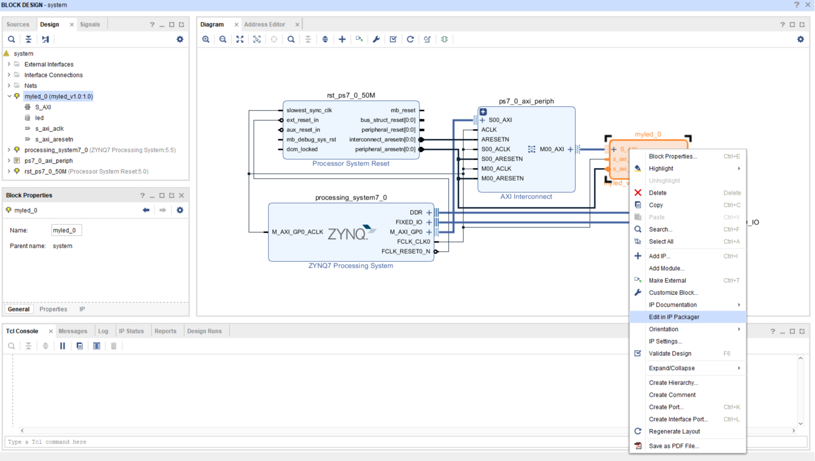
Right click on myled_0 in the diagram window and select Edit in IP Packager.
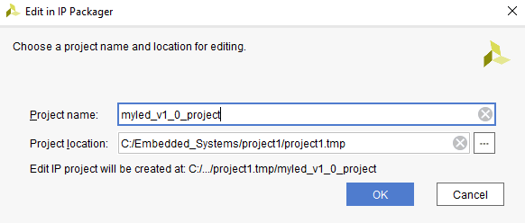
Vivado tools will create a special IP Edit project to handle the development and packaging an IP. A pop up dialog will appear at this point and ask you to set the name of this project and a location to store the project. You can just keep the default value here.
Open the top module myled_v1_0 from sources panel, and add a 4-bit wide output port named led to connect to on-board LEDs.
`timescale 1 ns / 1 ps

    module myled_v1_0 #
    (
        // Users to add parameters here

        // User parameters ends
        // Do not modify the parameters beyond this line


        // Parameters of Axi Slave Bus Interface S_AXI
        parameter integer C_S_AXI_DATA_WIDTH	= 32,
        parameter integer C_S_AXI_ADDR_WIDTH	= 4
    )
    (
        // Users to add ports here
        output wire [3:0] led,
        // User ports ends
        // Do not modify the ports beyond this line


        // Ports of Axi Slave Bus Interface S_AXI
        input wire  s_axi_aclk,
        input wire  s_axi_aresetn,
        input wire [C_S_AXI_ADDR_WIDTH-1 : 0] s_axi_awaddr,
        ...
Within top module myled_v1_0, a myled_v1_0_S_AXI is instantiated with name myled_v1_0_S_AXI_inst. As the comments above the module instantiation reads, it implements the AXI Bus Interface. The implementation is in file myled_v1_0_S_AXI.v. Please read the Verilog codes in the file, as well as the comments surrounding the codes.
When the ARM processor issues load and store instructions to access myled controller, signals on AXI bus will be toggled accordingly, and eventually, the data will be written to or read from slv_reg0, slv_reg1, slv_reg2, slv_reg3. The default memory mapping of those registers is shown in the table below.
| Address | Signal Name |
|---|---|
| 0x4BB00000 | slv_reg0 |
| 0x4BB00004 | slv_reg1 |
| 0x4BB00008 | slv_reg2 |
| 0x4BB0000C | slv_reg3 |
As there are only 4 on-board non-RGB LEDs, you only need to wire out the lowest 4-bits of slv_reg0 to the output port led of the top module myled_v1_0.
In order to do so, you need to create a 4-bit wide output port in module myled_v1_0_S_AXI called led, as shown below.
module myled_v1_0_S_AXI #
(
    // Users to add parameters here

    // User parameters ends
    // Do not modify the parameters beyond this line

    // Width of S_AXI data bus
    parameter integer C_S_AXI_DATA_WIDTH	= 32,
    // Width of S_AXI address bus
    parameter integer C_S_AXI_ADDR_WIDTH	= 4
)
(
    // Users to add ports here
    output wire [3:0] led,
    // User ports ends
    // Do not modify the ports beyond this line

    // Global Clock Signal
    input wire  S_AXI_ACLK,
    // Global Reset Signal. This Signal is Active LOW
    input wire  S_AXI_ARESETN,
    ...
Then use slv_reg0 to drive led port with an assign statement
    ...
    // Add user logic here
    assign led = slv_reg0[3:0];
    // User logic ends

    endmodule
Finally, connect port led of module myled_v1_0_S_AXI_inst to the top module output port led in file myled_v1_0.v.
    // Instantiation of Axi Bus Interface S_AXI
    myled_v1_0_S_AXI # (
        .C_S_AXI_DATA_WIDTH(C_S_AXI_DATA_WIDTH),
        .C_S_AXI_ADDR_WIDTH(C_S_AXI_ADDR_WIDTH)
    ) myled_v1_0_S_AXI_inst (
        .led(led),
        .S_AXI_ACLK(s_axi_aclk),
        .S_AXI_ARESETN(s_axi_aresetn),
        .S_AXI_AWADDR(s_axi_awaddr),
        .S_AXI_AWPROT(s_axi_awprot),
        ...
After wiring out slv_reg0[3:0] to led port, you need to add the port led in the IP packager so that vivado tools know that there is a new output port in myled IP when the IP is inserted in the design. To update IP information, open Package IP tab, select Ports and interfaces section, and click Merge changes from Ports and Interface Wizard.
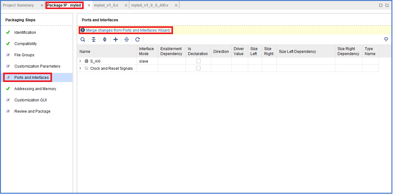
After this step, you will see port led is added to Ports and Interfaces list. Then you can select File Groups section, and click Merge changes from File Groups Wizard. You can click on Run Synthesize to synthesize the IP and make sure that your Verilog code has no errors and can be synthesized by the tools.
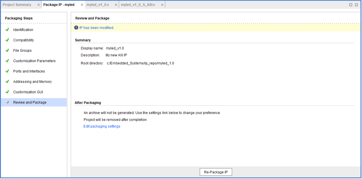
After you thoroughly checked your IP code, you need to re-package the IP core by selecting Review and Package section in Package IP tab. Click on button Re-Package IP and then close the edit IP project.
Update Myled IP in the Project
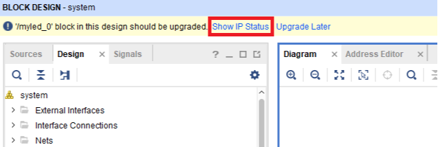
After port led is added to myled IP, the myled IP in original block diagram is not up to date. Thus, returning to project1 window, the vivado tool should inform you that /myled_0 block in your design should be upgraded. Click on the Show IP Status link.
If after returning to project1 window, the vivado tool doesn’t inform you that /myled_0 block in your design should be upgraded, you need to find an empty space in your block diagram, right click and select Validate Design. After this Show IP Status link should appear as shown in figure 25.
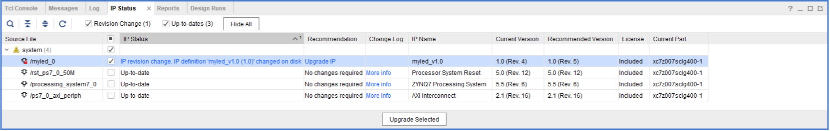
In the IP Status panel at the bottom of the window, select /myled_0 from the list, and click button Upgrade Selected to upgrade myled IP instance.
No Response After Clicking Upgraded Selected Button?
After click the button Upgrade Selected, the /myled_0 block in the block diagram should have an output port named
led. However, if nothing happened, you may want to check and see if you have saved your block diagram or not. If there are unsaved changes in your block diagram, Vivado may refuse and ignore the IP upgrade request. To solve that, just save the block diagram via the Save button in the tool bar, or with the Ctrl + s key combination.
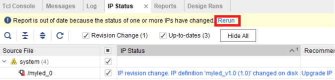
In the IP Status an option to Rerun the report appears. Press Rerun to update the report and the IPs within it.
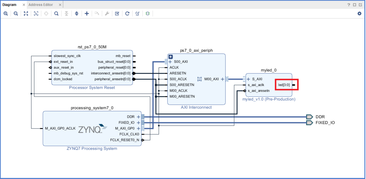
After the IP is upgraded, Generate Output Products dialog window will pop up, you may skip it for now. Then you will see output port led on block myled_0 in the diagram.
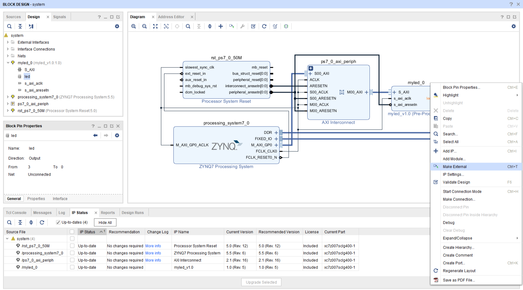
Make led Port External
In order to make connection between port led of block myled_0 to on-board LEDs, port led needs to connect to external output ports in system block diagram. Right click on port led and select Make External.
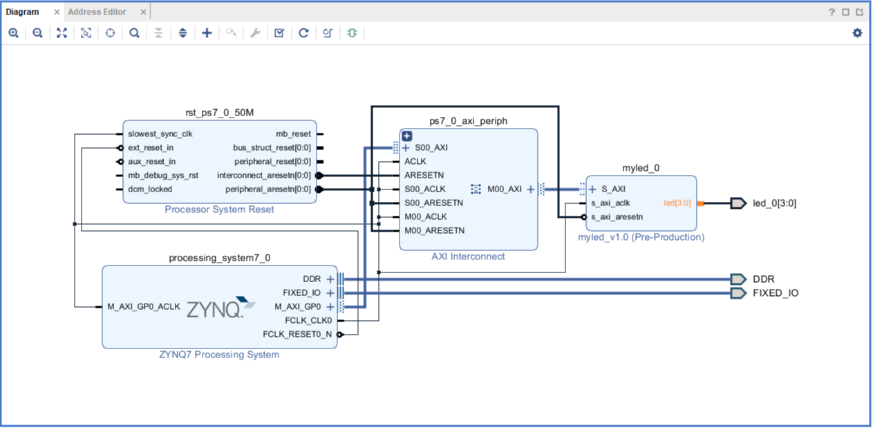
Check System Block Diagram
After all the steps, you have finished implementing your custom LED controller and connecting it to the ARM processor. Please compare your block diagram with the diagram below to make sure your connections look similar.
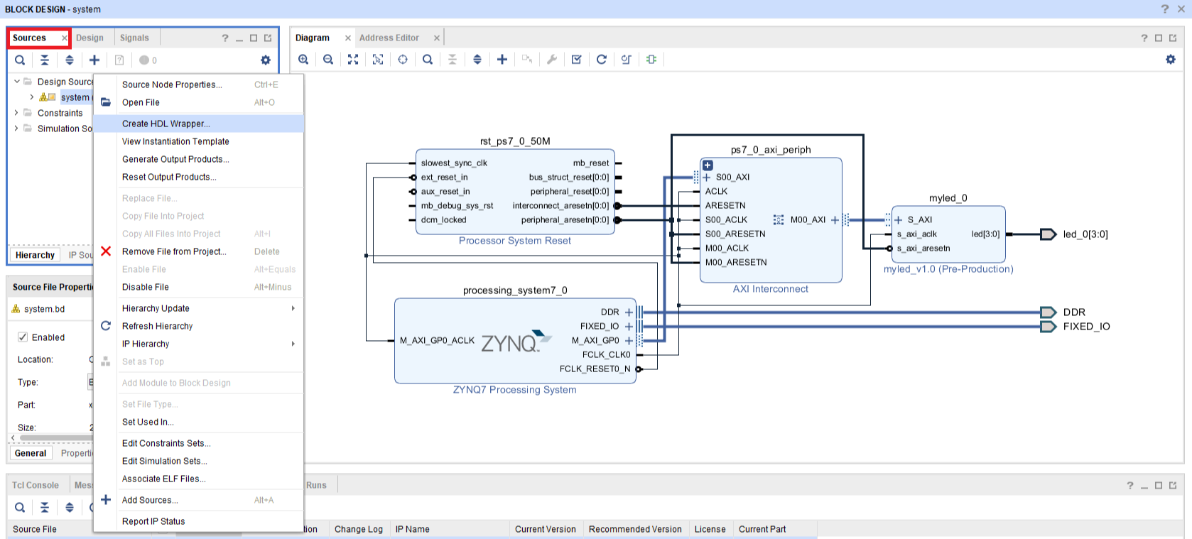
Generate HDL Wrapper
Instead of writing the top level HDL file for the block design yourself, vivado can create that file in Verilog for you. Select Sources tab on top left corner of Block Design window. Right click on system and select Create HDL Wrapper.
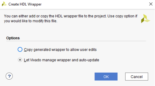
In the pop up dialog, select Let Vivado manage wrapper and auto-update, and click OK.
Critical Warning about DDR DQS_TO_CLK Delay
When you create the wrapper for the design, several critical warnings regarding negative DDR DQS_TO_CLK delay may occur. Since the DDR interface controller is configured with DDR training enabled, you can ignore those critical warning. However, at times, you may need to run synthesize or implementation twice, and Vivado will ignore those critical warnings. Please see this Xilinx forum thread for more details.
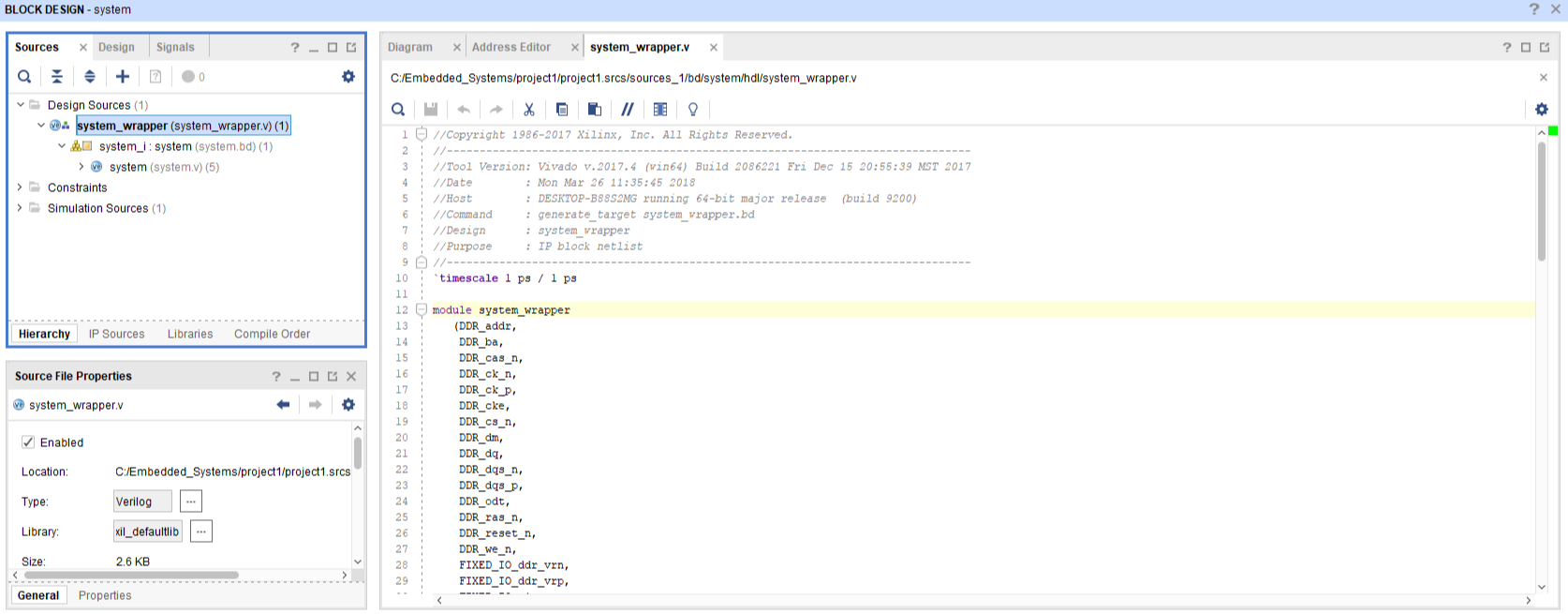
Now, a system_wrapper.v file is generated and it is listed as top module under source panel. Double click and open the file, you can see the input and output ports of the generated top module as follows:
`timescale 1 ps / 1 ps
module system_wrapper
   (DDR_addr,
    DDR_ba,
    DDR_cas_n,
    DDR_ck_n,
    DDR_ck_p,
    DDR_cke,
    DDR_cs_n,
    DDR_dm,
    DDR_dq,
    DDR_dqs_n,
    DDR_dqs_p,
    DDR_odt,
    DDR_ras_n,
    DDR_reset_n,
    DDR_we_n,
    FIXED_IO_ddr_vrn,
    FIXED_IO_ddr_vrp,
    FIXED_IO_mio,
    FIXED_IO_ps_clk,
    FIXED_IO_ps_porb,
    FIXED_IO_ps_srstb,
    led);
  inout [14:0]DDR_addr;
  inout [2:0]DDR_ba;
  inout DDR_cas_n;
  inout DDR_ck_n;
  inout DDR_ck_p;
  inout DDR_cke;
  inout DDR_cs_n;
  inout [3:0]DDR_dm;
  inout [31:0]DDR_dq;
  inout [3:0]DDR_dqs_n;
  inout [3:0]DDR_dqs_p;
  inout DDR_odt;
  inout DDR_ras_n;
  inout DDR_reset_n;
  inout DDR_we_n;
  inout FIXED_IO_ddr_vrn;
  inout FIXED_IO_ddr_vrp;
  inout [53:0]FIXED_IO_mio;
  inout FIXED_IO_ps_clk;
  inout FIXED_IO_ps_porb;
  inout FIXED_IO_ps_srstb;
  output [3:0]led;
Add Physical Constraints
In all the outputs listed in system_wrapper module, led belongs to PL part and needs physical constraints to tie them to actual pins on FPGA. So, here you need to create a xilinx design constraint (XDC) file to inform Vivado which pins are connected to on-board LEDs.
Right click on constraints in the Sources panel and select Add Sources
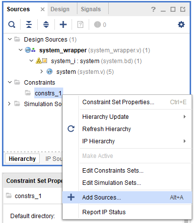
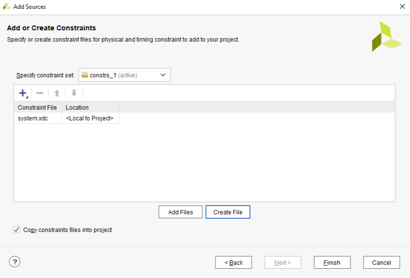
In the pop-up Add Sources dialog, select Add or Create Design Constraints and click Next.
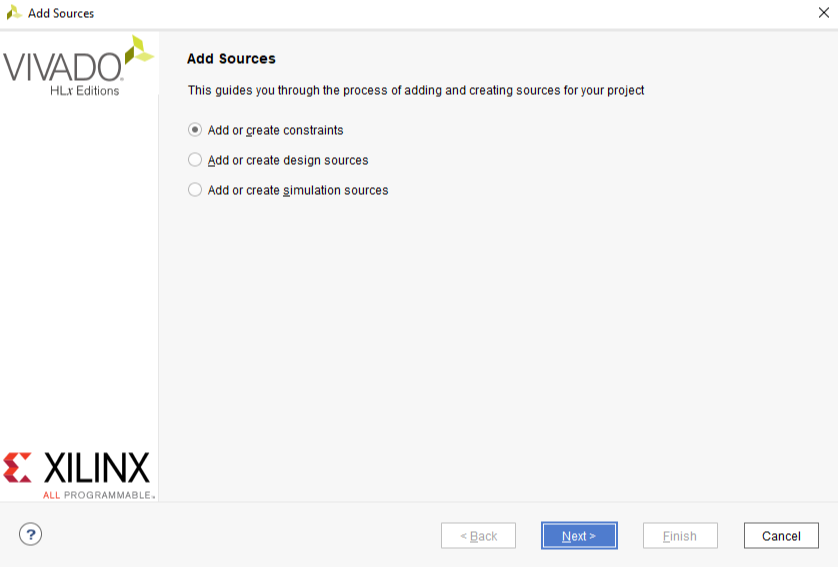
Click Create File button and just name the file system. Click Finish to finish creating and adding the new constraint file system.xdc into the project.
Now, we need to put down the physical constraints for 4 led ports.
##LEDS
#IO_L14P_T2_SRCC_34 Schematic name=LD0
set_property -dict { PACKAGE_PIN N20   IOSTANDARD LVCMOS33 } [get_ports { led[0] }];
#IO_L14N_T2_SRCC_34 Schematic name=LD1
set_property -dict { PACKAGE_PIN P20   IOSTANDARD LVCMOS33 } [get_ports { led[1] }];
#IO_0_34 Schematic name=LD2
set_property -dict { PACKAGE_PIN R19   IOSTANDARD LVCMOS33 } [get_ports { led[2] }];
#IO_L15P_T2_DQS_34 Schematic name=LD3
set_property -dict { PACKAGE_PIN T20   IOSTANDARD LVCMOS33 } [get_ports { led[3] }];
Where to find information about I/O Constraints
You can find the location you need from the schematic of your FPGA board and marked by the switches or LEDs on your board, or you can download the master XDC for your Blackboard Blackboard master XDC and copy the corresponding lines for this step.
You’ve now successfully prepared the hardware design!
Preparing the hardware design includes creating a block design, making a custom AXI4-Lite IP, generating an HDL wrapper, and setting up Physical Constraints.