Structural Implementation of an Asynchronous Counter
Structural Verilog using Xilinx flip-flop primitives

Structural Verilog techniques can be useful when preexisting circuit blocks can be reused in a new design. Xilinx makes many basic components available in the Vivado tool, including D-FF’s. Here, we present an asynchronous counter built from Xilinx flip-flop primitives.
Recall that structural Verilog builds a circuit by interconnecting preexisting circuit components. A component is instantiated in a Verilog file by including its name, and then listing all the port connections. An example is presented below. The component called “simple” is instantiated and used in the higher-level design called “next”. In the module next, the component simple is instantiated by including its name, followed by a port-connection list in parenthesis. In the port connection list, the component name is written first, immediately after a period, and then the higher-level port to which it connects is shown in parenthesis.

For this asynchronous counter design, the Xilinx flip-flop primitive called “dff_inst0” can be used. The Verilog code below shows how this component can be instantiated in a Verilog source file.
dff dff_inst0 (
    .clk(clk),
    .rst(rst),
    .D(din[0]),
    .Q(clkdiv[0])
);
The clock divider in this design receives a 100MHz clock, and it must produce a clock that toggles at less than 1Hz – this requires 27 flip-flops (since 100MHz / 2^27 is .745Hz). The figure below shows the circuit.

To create this circuit, you could instantiate 27 copies of the DFF Verilog code above, and then manually connect all the clock signals between neighboring flip-flops. Or, you can use a Verilog for loop to automatically “tile out” the flip-flops for you. The for loop can create copies of the flip-flop, and we can create busses to define the input and output signals between the flip-flops.
genvar i;
generate
for (i = 1; i < 27; i=i+1)
begin : dff_gen_label
    dff dff_inst (
        .clk(clkdiv[i-1]),
        .rst(rst),
        .D(din[i]),
        .Q(clkdiv[i])
    );
    end
endgenerate
In the code below, the flip-flop 0 is instantiated on its own, and then the for loop creates the remaining 26. Note the “assign din = ~clkdiv” statement towards the bottom of the code listing – that statement inverts every flip-flop’s output before returning it to the input. The Verilog file for this design is below. Take the time to look through the code, and be sure you understand what’s happening.
`timescale 1ns / 1ps
module clk_divider(
    input clk,
    input rst,
    output led
    );

wire [26:0] din;
wire [26:0] clkdiv;

dff dff_inst0 (
    .clk(clk),
    .rst(rst),
    .D(din[0]),
    .Q(clkdiv[0])
);

genvar i;
generate
for (i = 1; i < 27; i=i+1)
begin : dff_gen_label
    dff dff_inst (
        .clk(clkdiv[i-1]),
        .rst(rst),
        .D(din[i]),
        .Q(clkdiv[i])
    );
    end
endgenerate

assign din = ~clkdiv;

assign led = clkdiv[26];

endmodule
A Test Bench to Simulate the Clock Divider Circuit
As with the combinational circuit we have designed in previous projects, you can draft a test bench to test the circuit out before implementing it on-chip. However, in this test bench, we need to emulate the clock signal and the rst signal. The clock signal is actually a constantly oscillating signal. Using the Blackboard as an example, the input clock frequency is 100 MHz, i.e., the period of the clock is 10 ns. Half of the period the clock is high, half of the period clock is low. In other words, every half of the period, 5 ns in this case, the clock will flip itself. To simulate the clock signal, instead of putting it in the initialize statement, we will use an always statement.
`timescale 1ns / 1ps

...

reg clk;

always
    #5 clk = ~clk;
In the initialize block, we will initialize clk signal to 0 and hold rst high for 10ns to reset the clock divider. So, the Verilog Test Bench will look like this:
`timescale 1ns / 1ps

module tb;

    // Inputs
    reg clk;
    reg rst;

    // Outputs
    wire led;

    // Instantiate the Unit Under Test (UUT)
    clk_divider uut (
        .clk(clk),
        .rst(rst),
        .led(led)
    );

    always
        #5 clk = ~clk;

    initial begin
        // Initialize Inputs
        clk = 0;
        rst = 1;

        #10 rst = 0;

        // Wait 100 ns for global reset to finish
        #100;

    end

endmodule
Simulating the Clock Divider
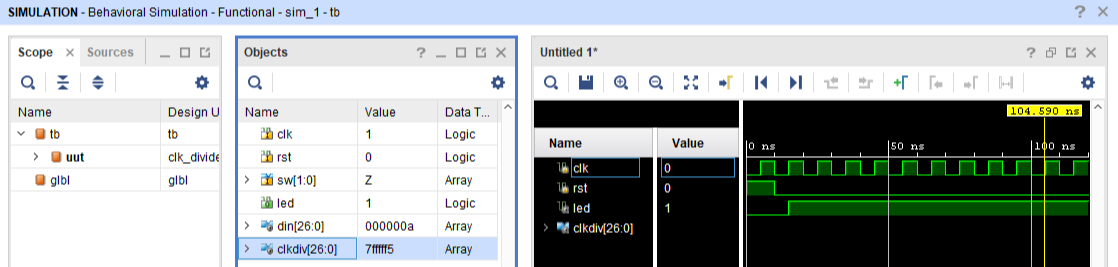
When you first run behavioral simulation, the internal signals such as clkdiv[26:0] won’t appear in the simulation window. You can access these signals by opening windows Scope and Objects on the left side of the simulation window and clicking on uut under Scope window. Now you can see clkdiv[26:0] under Objects window, go ahead and click and drag this signal to the simulation window under the Name column as show in figure 3. You can also drag clkdiv[26:0] signals into the simulation window one by one in any order you want.
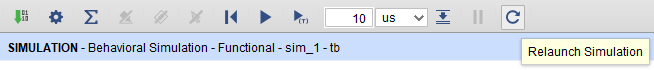
Now you have clkdiv[26:0] in your simulation window, but it doesn’t have any signals. In order to see those signals, you need to relaunch your simulation by clicking Relaunch Simulation icon  as shown in figure 4. You can also achieve the same result by clicking on Restart icon
  to restart the simulation and then clicking on Run All icon
  to start the simulation again, both of which can be found on the same toolbar as the Relaunch Simulation icon.
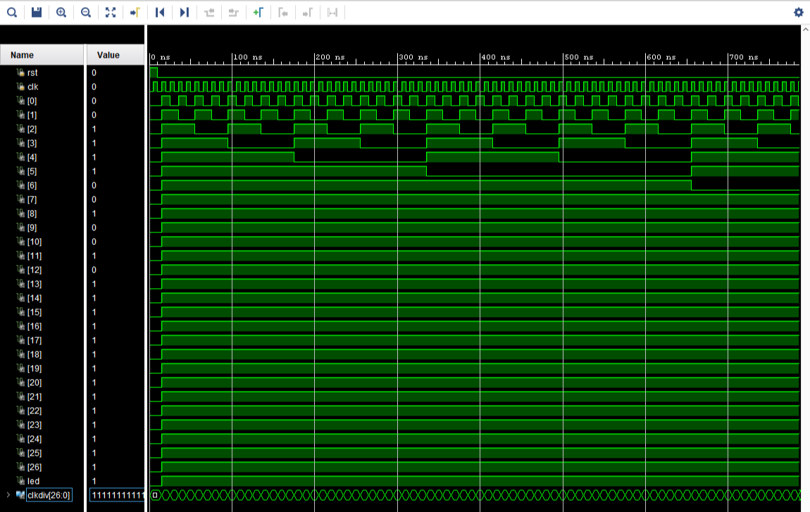
The simulated waveform is shown in Fig. 5 below. You can see in the waveform that clkdiv[0] is half of the frequency of clk, and that clkdiv[1] is half of the frequency of clkdiv[2].