The design of a Majority of Five circuit
An illustrated design process with an introduction to simulation

This tutorial steps through the design of a five-input circuit that detects when three or more inputs are asserted. The truth table below formalizes the requirement, and the same information is shown in the uncompressed “super K-map” and in an entered-variable K-map. Optimal equations can be looped from either the super map or EV map – an initial set of loops is shown.

All the terms in the final equation will have three logic variables, and all unique three-variable terms will be included in the equation (why?). A “5 choose 3” calculation shows there are 10 ways to choose three variables out of five; it follows that ten 3-input terms can be defined from a pool of five input variables. You can find the terms through looping, or perhaps you can discern them just by thinking through the combinations. Either way, the Verilog code below captures the requirement. Pause a moment to think about this, and make sure you agree and understand.
module majority_of_five(input [4:0] sw, output led);

assign led =	(sw[0] & sw[1] & sw[2]) | //ABC
		(sw[0] & sw[1] & sw[3]) | //ABD
		(sw[0] & sw[1] & sw[4]) | //ABE
		(sw[0] & sw[2] & sw[3]) | //ACD
		(sw[0] & sw[2] & sw[4]) | //ACE
		(sw[0] & sw[3] & sw[4]) | //ADE
		(sw[1] & sw[2] & sw[3]) | //BCD
		(sw[1] & sw[2] & sw[4]) | //BCE
		(sw[1] & sw[3] & sw[4]) | //BDE
		(sw[2] & sw[3] & sw[4]);  //CDE
endmodule
Simulator Overview
When Verilog source files are first created for more complex problems, it is quite possible (likely?) they contain some errors. Before implementing the design in hardware, or using it as a component in some other design, it makes good sense to use a logic simulator to check the circuit’s performance, and to verify that expected outputs are generated for all possible combinations of inputs.
You should adopt the habit of simulating your code and verifying your circuit’s performance as soon as the source code is complete. If you start using the simulator now, with simpler circuits, you will develop some amount of proficiency. Then, as your designs become more complex, running the simulator will not feel burdensome. Like thousands of engineers before you, you will find that if you simulate and verify your code early in the design process, you will decrease your work and increase your productivity.
The simulation process requires two source files – the Verilog code to be simulated, and a separate Verilog source file called a test bench to drive the simulator inputs. A test bench is a proper Verilog source file that can only be used to drive a simulator. It calls out or “instantiates” the Verilog source file to be simulated (often called the “Circuit Under Test, or CUT), it drives all the inputs to the CUT, and it defines how the inputs change over time. For example, a test bench to simulate a three input, one output CUT would contain statements to drive the inputs through all eight possible combinations, as well as statements to let some amount of simulator time pass between each input change so the output has time to attain its new value.
A Verilog test bench file is organized slightly differently than a design source file, and it can use certain statements that are not intended for synthesis (and so cannot be used in a design source file). A test bench is similar in appearance to a Verilog source file, but there are a few differences:
- The module statement has an empty port list;
- The Verilog module to be tested (the “Circuit Under Test”, or CUT) must be instantiated as a component in the test bench;
- All CUT input signals must be declared as type reg so the test bench can drive them;
- All output busses must be declared as type wire so they will be added to the simulator output waveform viewer;
- An “initial block” is used to contain assignment statements that drive the CUT inputs so they will be executed sequentially;
- Delay statements are used to force simulator time to pass.
In Vivado, a test bench file is created and edited just like any other Verilog file, but a “simulation source” file is created instead of a “design source” file. Vivado places test bench files in the Simulation Sources area in the Project Manager to keep them distinct from design source files. Once the test bench is complete, you can execute it by clicking on the Run Simulation link in the Flow Navigator. When the simulator starts, it will apply the inputs you defined to the CUT, let simulator time pass according to the statements in your source file, and report output signals to a “waveform viewer” where you can inspect them.
Creating a Test Bench
To create a test bench file, click on the Add Sources link in the Project Manager, but this time, select “Add or create simulation sources”. In the Add Sources dialog box that opens, click Create File, and select a meaningful file name for your testbench. It is common to incorporate the name of the file being tested in the test bench name. In this example, the source file as called “majority_of_five”, and so the test bench was called “majority_of_five_tb”. You are free to choose any names you wish, but consider adopting names that are significant in some way.

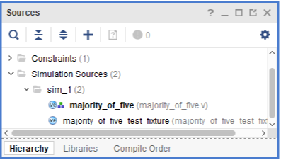
Once the test bench file is created, it will be listed under Simulation Sources in the Project Manager sources tab. Expand this section and double click the file you just created. Just like the Verilog design source files you have created, this new test bench file will contain a template. You can delete everything in this file, or keep the module name if you wish.
Time Scale
The first line of the test fixture should contain the timescale. You may recognize this line from the other Verilog files you have created.
`timescale 1ns/1ps;
The 'timescale directive defines the reference time and precision used by simulator. The code above defines a 1 ns reference time unit, and a 1 ps precision. The reference time is used by the simulator to determine the simulator “time step size”. You can include delay commands in your test bench to tell the simulator how many time steps to let pass. For example, the command #50 would direct the simulator to let 50 reference time units pass (50 ns in this case). The precision defines the smallest amount of time the simulator can represent. It becomes pertinent when more precise timing and delay simulations are needed - we’ll get to that in a later module.
An empty module statement is the first line in the test bench. You can name the module anything you like, but it is common to give it a relavant/meaningful name. Here, it is given the same name as the source file that contains it.
The next line declares all CUT input signals as type reg. These inputs will be driven by assignment statements in the test bench, and they must be delcared as regs so they can be assigned values in the “initial block” that follows. (Breifly, input signals into the CUT must be “variables” so they can be assigned inside a procedural block. They must be assigned in a procedural block so their values can be assigned sequentially over time. In Verilog, variables must be of type reg - this is all explained more fully in the Verilog topic documents.)
The next line declares outputs that will be shown the waveform viewer as wires. Note that individual output signals from the CUT will automatically be shown regardles of whether they are declaed as wires, but busses will not be shown unless they are declared as wires.
module majority_of_five_tb;

    // Inputs
    reg [4:0] sw;
    // Outputs
    wire led;
Next, the CUT must be instantiated. In the statement below, the name of the CUT appears first (majority_of_five), followed by a text string to name the instantiation. This text string can be anything - it is typical to name it something like “cut” for circuit under test. The “port list” follows the instantiation name. In the port list, the name of the instantiated signal pin is prepended with a period (.), and it is immediately followed by the name of the top-level signal it connects to, in parenthesis. So for example, if an input signal to the CUT is named X, and it is to be driven from a test bench signal called Y, the format would be .X(Y). Often, the signals in the test bench are given the exact same names as the signals in the CUT, so the mappings are clear. For example, if an input signal to the CUT is named X, the test bench signal that drives it could also be named X, and the format would be .X(X).
In the statement below, the input signals to the CUT called sw are connected to the test bench signals called sw that were declared above in the reg statement, and the output signal from the CUT is connected to the test bench signal led.
majority_of_five cut (.sw(sw), .led(led));
The rest of the test bench file contains assignment statements to drive input signals, and delay statements to direct the simulator to let time pass. All statements are contained inside an “initial” block so they will be executed in the order they appear.
Assignment statements name the signal to be assigned, followed by an equal sign, followed by the intended value (1 or 0). Delay statements use the # sign followed by a number of time steps. Consider a circuit with three inputs A, B, and C. The following lines would assign all 0’s to the inputs, allow 10 time steps to pass, then assign 0, 0, 1, then allow 10 time steps to pass, then assign 0, 1, 0, then 10 time step, all the way to 1, 1, 1.
Assigning 10 time steps to pass between input assertions is somewhat common but also somewhat arbitrary – you could choose any number. In general, choosing a large number means the simulation must run for a longer time, and choosing a small number limits the time the simulator has to resolve signal changes (but that is not a factor until the simulator uses delay values – we’ll get to that around chapter 6).
initial begin
	A = 0; B = 0; C = 0;
	#10
	A = 0; B = 0; C = 1;
	#10
	A = 0; B = 1; C = 0;
	#10
	A = 0; B = 1; C = 1;
	#10
	A = 1; B = 0; C = 0;
	#10
	A = 1; B = 0; C = 1;
	#10
	A = 1; B = 1; C = 0;
	#10
	A = 1; B = 1; C = 1;
	#10
end
Defining signal values directly as shown above is straight-forward, but it gets time consuming for large numbers of inputs. In this case, we have five inputs, and so we’d need to type 32 lines of assignment statements, with each line assigning values to all five inputs.
More compact code can be written using a for loop. A Verilog for loop works like a C for loop, and the syntax is shown below. The index variable k is declared as an integer, and integers are represented in Verilog as 32-bit numbers. The bits in the index variable k can be directly assigned to the sw inputs using a single assignment statement. This causes the least-significant bit of k to be assigned to the least significant bit of sw, and then the next least significant bits are assigned, and so on until there are no more sw inputs.
The “$finish” directive at the end directs the simulator to stop. If that directive is not included, the simulator will stop after no inputs have changed state for a period of time.
// Declare loop index variable
integer k;

// Apply input stimulus
initial
begin
    sw = 0;

    for (k=0; k<32; k=k+1)
        #20 sw = k;

    #20	$finish;
end
Finally, close the module as usual with endmodule. The completed test bench should look like the following:
`timescale 1ns/ 1ps

module majority_of_five_tb;

// Inputs
reg [4:0] sw;
// Outputs
wire led;

// Instantiate the Circuit Under Test (CUT)
majority_of_five cut (.sw(sw),.led(led));

// Declare loop index variable
integer k;

// Apply input stimulus
initial
begin
    sw = 0;

    for (k=0; k<32; k=k+1)
        #20 sw = k;

    #20	$finish;
end
endmodule
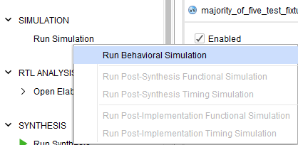
Run Behavioral Simulation
Once the test bench is complete, the simulator can run. Under the Simulation heading in theFlow Navigator, select Run Behavioral Simulation. This will launch the simulator, drive the CUT with the defined inputs, and open the waveform view window to display the results.
Check Waveform in Simulator
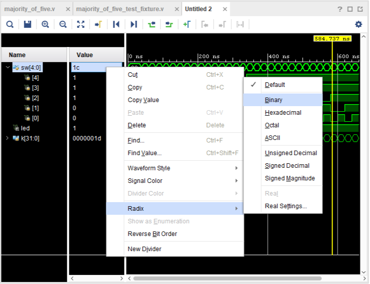
After the simulation runs, the Behavioral Simulation window will appear. Select the tab with an untitled name. Your simulation should look like the image shown in the figure.
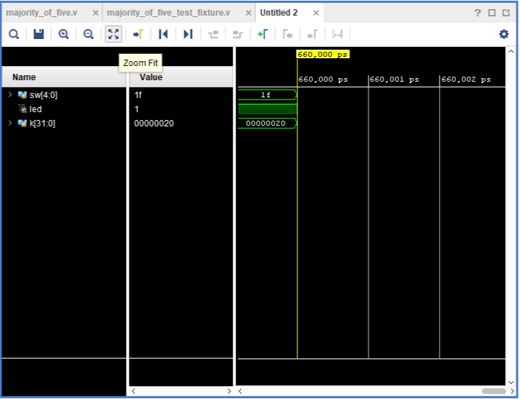
In order to see the full simulation shown in the image below, you will need to click Zoom fit icon  to zoom fit the simulation. Use the zoom keys (+ and - inside magnifying glasses) to zoom in or out - if you zoom in to the sw signal changes, you will be able to see the changing values of the switches as a waveform.
You can also “pull” a cursor from the left side of the waveform view window (the yellow line in the figure) and this will show the current values. Notice where the cursor is in the image below: sw 4 through 2 are high, so led is high. You should look through all the input patterns and make sure that the output signal works as expected.
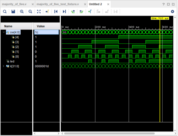
You can change how the values in the simulation window are displayed by right-clicking on a signal name and choosing a different radix. In the figure, the sw[4:0] signal value is being changed to display as a binary number.