AXI4-Lite Read/Write Transaction at Runtime
Using Debug (ILA - Integrated Logic Analyzer) on AXI4-Lite Bus

Scope AXI4-Lite Read/Write Transaction at Runtime
To understand how AXI4-Lite works, nothing is better than scoping it while it is running. In this section, you will use chipscope to scope the AXI4-Lite read and write transaction to your myled custom IP core when it is running on your board.
Step 1: Open LED Controller Project
Open Vivado tools menu, and click on Open Existing Projects. Navigate to myled project and open the project. Then open the block design as show in figure 1.
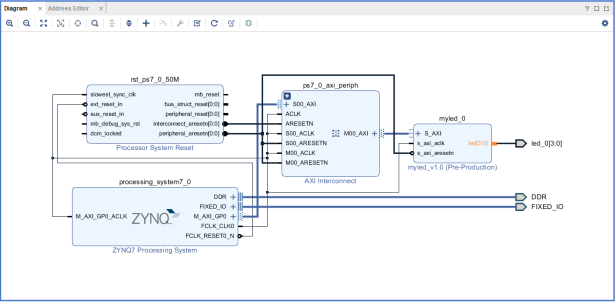
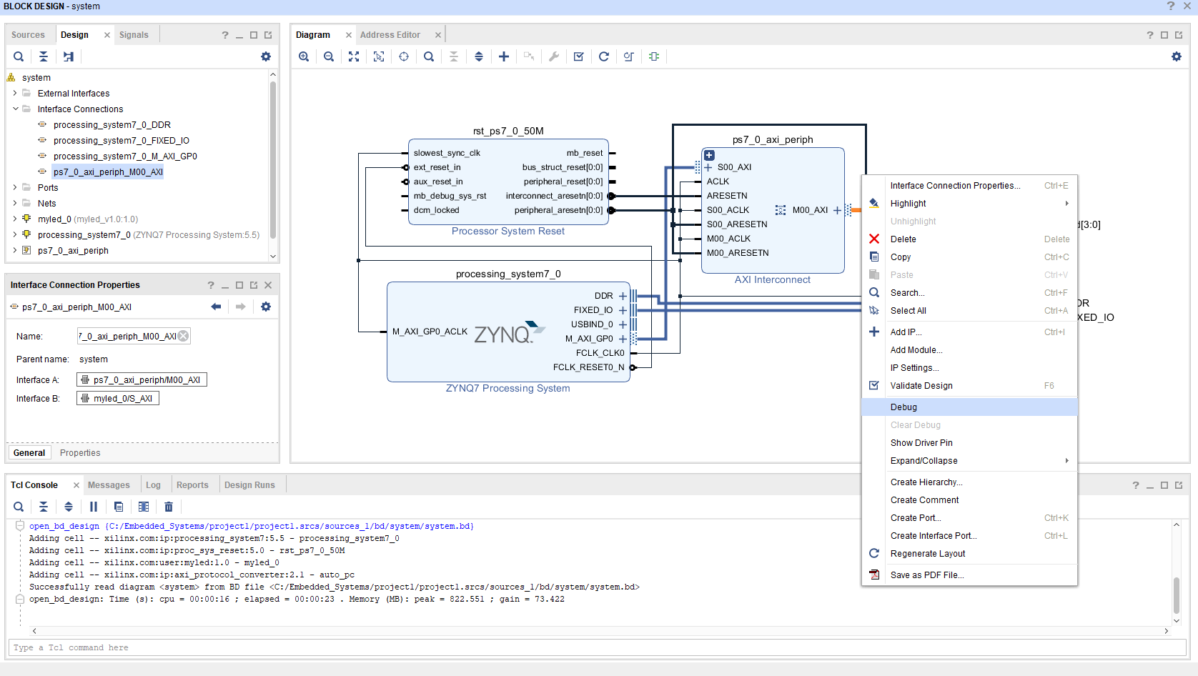
Step 2: Add Debug on AXI Bus of myled IP Core
Select the AXI Bus of myled IP Core. Then right click on the selected AXI bus, and select Debug in the drop down menu.
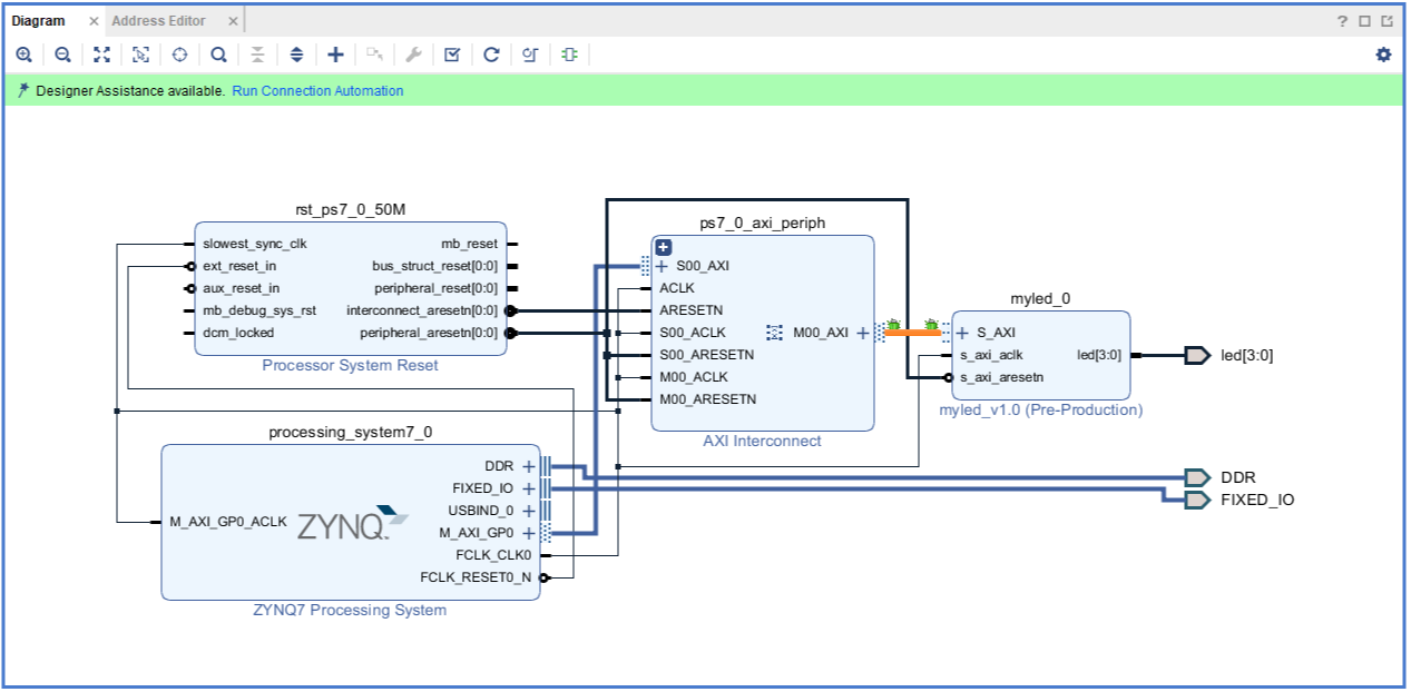
You should see the debug icon labeled on the marked AXI bus.
You can mark signal as debug in Verilog as well
If you want to scope an internal signal in your IP module, you can mark Debug in your Verilog code as well. In the codes below, you can also mark slv_reg0 with DEBUG property. Note that the KEEP property is usually marked together with DEBUG so that the synthesizer will not remove the signal during optimization.
//-- Number of Slave Registers 4
(* mark_debug = "true", keep = "true" *)
reg [C_S_AXI_DATA_WIDTH-1:0]    slv_reg0;
(* mark_debug = "true", keep = "true" *)
reg [C_S_AXI_DATA_WIDTH-1:0]    slv_reg1;
(* mark_debug = "true", keep = "true" *)
reg [C_S_AXI_DATA_WIDTH-1:0]    slv_reg2;
(* mark_debug = "true", keep = "true" *)
reg [C_S_AXI_DATA_WIDTH-1:0]    slv_reg3;
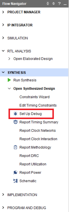
Step 3: Run Synthesis, Open Synthesized Design, and Add Logic Analyzer Core
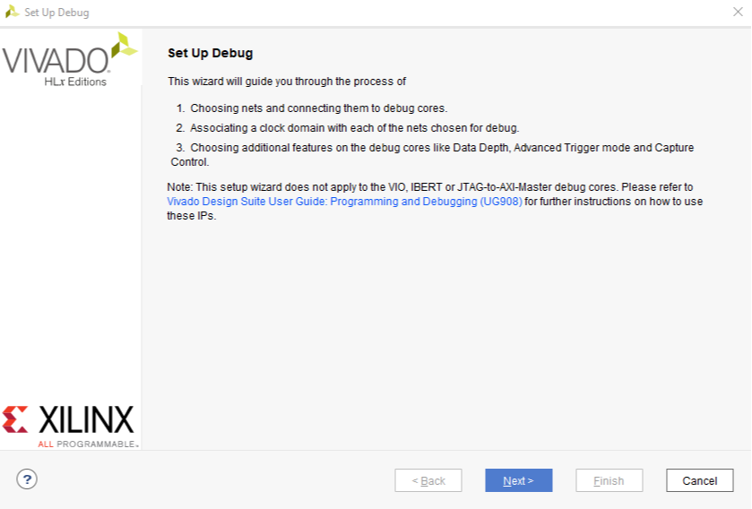
First Run synthesis then select Set Up Debug in the Flow Navigator window. You’ll be promted to open up the synthesized design, click YES.
A Set Up Debug dialog will pop up for you to selected signals to scope and insert a logic analyzer core into your system. Click Next.
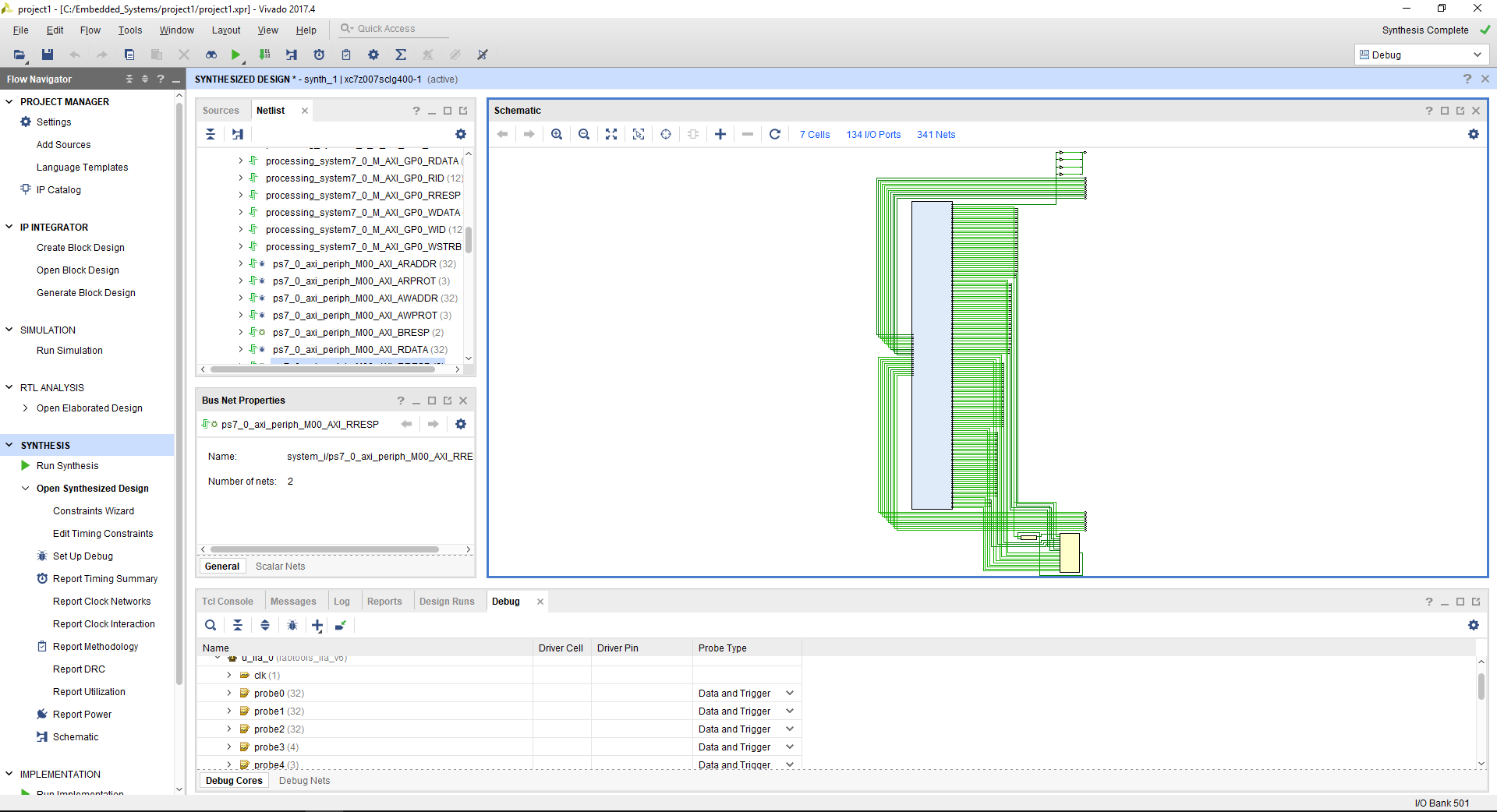
You will now see a dialog Nets to Debug window as shown in figure 6.
Note: If these Nets didn’t appear automatically in this window, click Find Nets to Add…. Then use drop down menu to change the filter property to MARK_DEBUG is true. You will now prompted with a dialog, select all signlas from there and click OK.
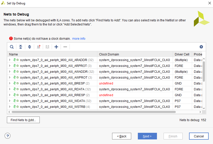
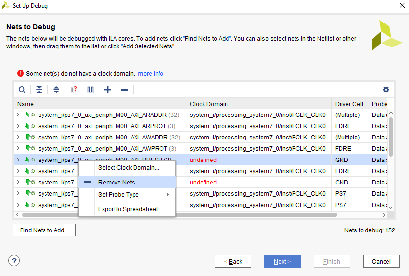
You will notice that the clock domain of signals system_i/ps7_0_axi_eriph_M00_AXI_BRESP and system_i/ps7_0_axi_eriph_M00_AXI_RRESP are undefined. This is because both signals are tied to ground (notice the GND in Driver Cell column) all the time. So, there is really no need to monitor those signals. Select them, right click and choose Remove Nets.
The the error message will go away and you can click Next to move on.
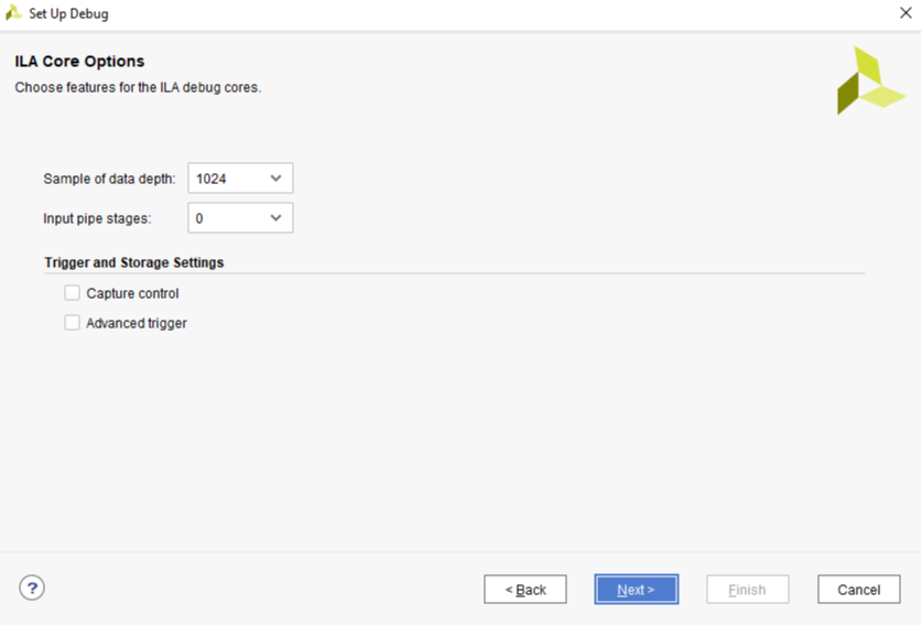
On ILA Core option page, you can select how many data the hardware should keep in its buffer. The depth of the sample data can be increase at the cost of more hardware resource consumption. In this lab, we can leave it at 1024.
For more details on the options, you can refer to UG908 Vivado Design Suite User Guide: Programming and Debugging for more information.
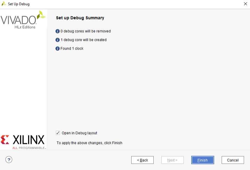
Now you will land on the summary page. Simply click Finish to close the Set Up Debug Dialog
Click on the Save button (or use key combination
As you have added logic analyzer to the hardware project, you will need to run implementation and bitstream generation. You also need to export your hardware to your SDK project again so that it is up-to-date.
Step 4: Scope AXI4-Lite Read/Write Transaction at Run-time
In order to assure that you can scope the signals complete these 3 sub-steps before continuing:
- Make sure you generted the bitstream and exported the hardware including the bitstream.
- Lanch SDK (don’t close Vivado)
- Program FPGA from SDK and run the software on the board
Now, switch back to Vivado project, and click on Open Hardware Manager to open hardware manager. Then click Open Target and autmtically connect to your Blackboard.
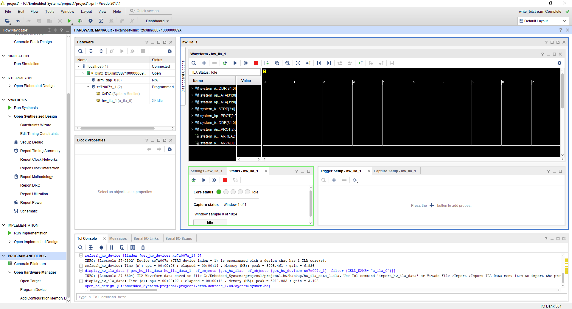
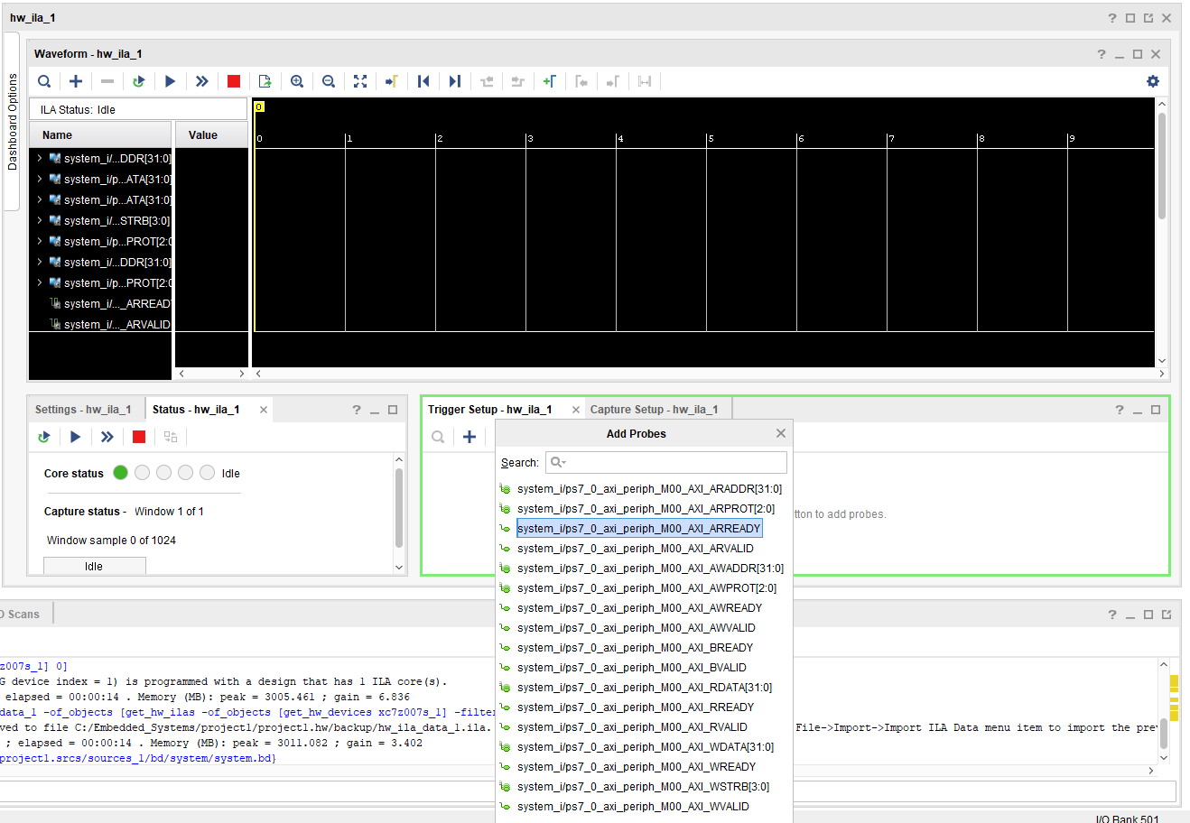
In the Trigger Setup panel, click the Add Probes button to add probes.
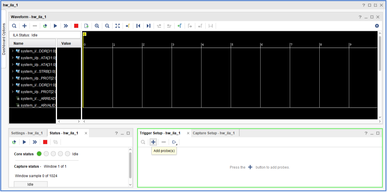
In the pop up window, select signal system_i/ps7_0_axi_periph_M00_AXI_ARREADY.
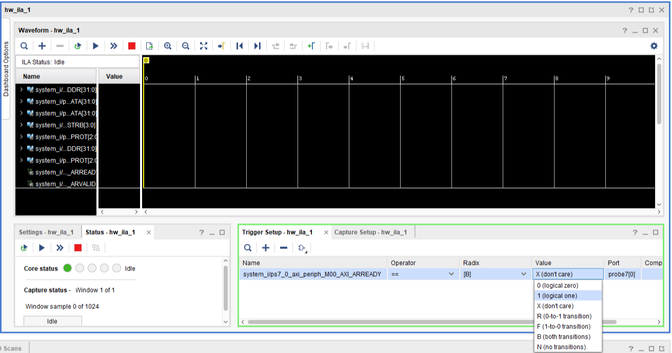
Set the logic analyzer triggered by the time ARREADY signal is logic 1.
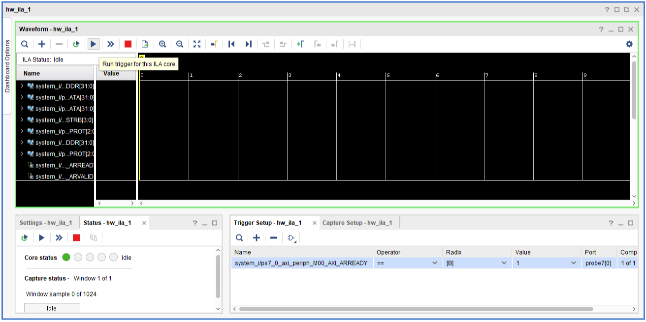
Click on the Play button to run trigger for this ILA core, and you will see the waveform window populated as soon as ARREADY jumps up to 1.
The following two figure shows the read/write transaction on AXI4-Lite bus using ILA debug core.

