Creating Your First Project in Vivado
Introduction to the Vivado Design Environment

This tutorial is intended to guide you through the creation of your first Vivado project. It covers:
- How to create a new project;
- How to edit a project and add required source files;
- How to Synthesize and Implement a project, and how to generate a bitstream;
- And finally, how to program your Real Digital board.
You may want to refer back to this tutorial over the course of the first few projects as you gain confidence with the Vivado tool - you will need to repeat these same general steps whenever you create a new project in the future.
Step 1: Create a Vivado Project
Vivado Projects
Vivado “projects” are directory structures that contain all the files needed by a particular design. Some of these files are user-created source files that describe and constrain the design, but many others are system files created by Vivado to manage the design, simulation, and implementation of projects. In a typical design, you will only be concerned with the user-created source files. But, in the future, if you need more information about your design, or if you need more precise control over certain implementation details, you can access the other files as well.
When setting up a project in Vivado, you must give the project a unique name, choose a location to store all the project files, specify the type of project you are creating, add any pre-existing source files or constraints files (you might add existing sources if you are modifying an earlier design, but if you are creating a new design from scratch, you won’t add any existing files – you haven’t written them yet), and finally, select which physical chip you are designing for. These steps are illustrated below.
Start Vivado
In Windows, you can start Vivado by clicking the shortcut on the desktop. In Linux, you can start Vivado using the command in the terminal as shown in TUTORIAL: VIVADO TOOLS INSTALLATION.
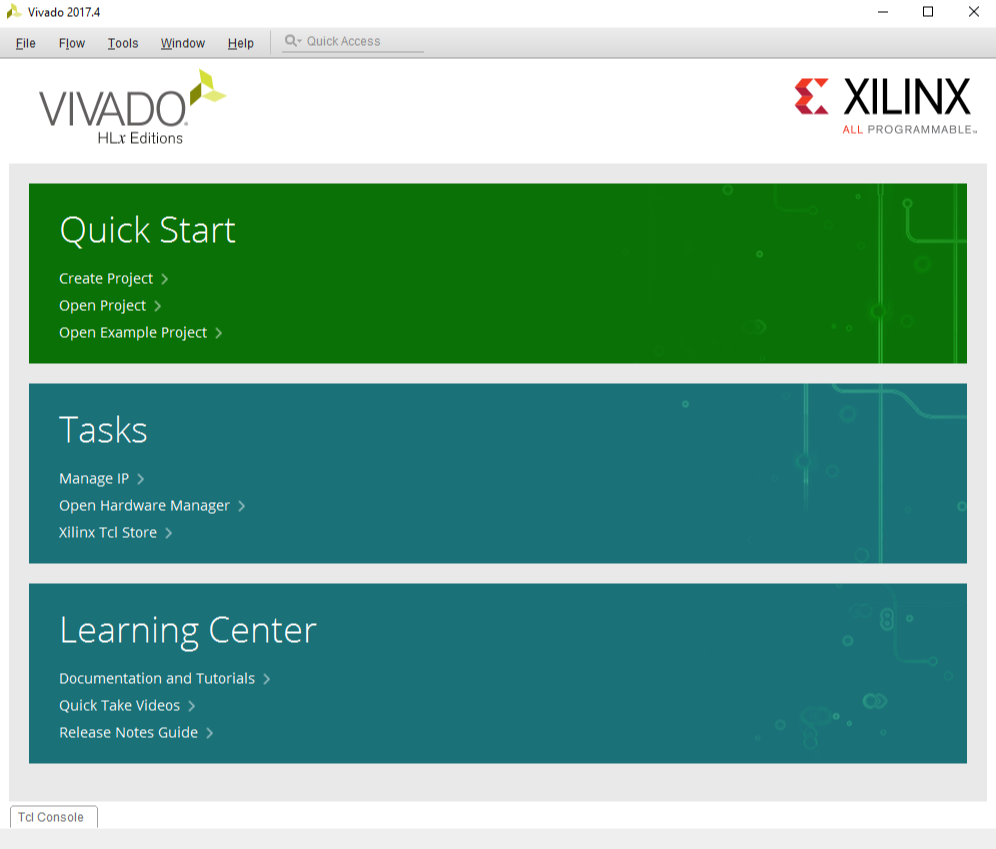
After Vivado is started, the window should look similar to the picture in figure 1.
Open Create Project Dialog
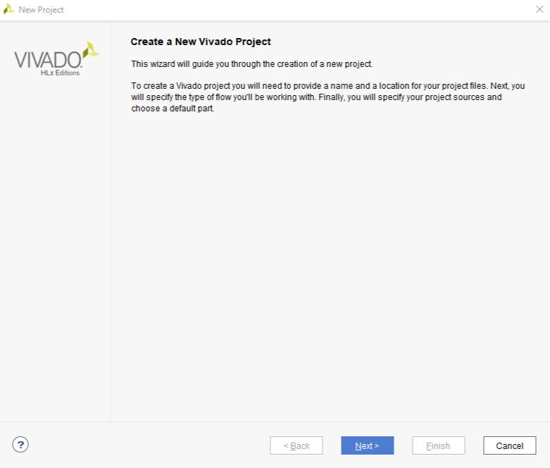
Click on “Create Project” in the Quick Start panel. This will open the New Project dialog as shown in Figure 2. Click Next to continue.
Set Project Name and Location
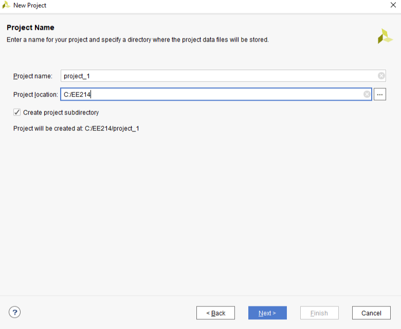
Enter a name for the project. In the figure, the project name is “project_1”, which isn’t a particulary useful name. It’s usually a good idea to make the project name more descriptive, so you can more readily identify your designs in the future. For example, if you design a seven-segment controller, you might call the project “seven segment controller”. For projects related to coursework, you might include the course name and project number - for example, “ee214_project2”. You should avoid having spaces in the project name or location, because spaces can cause certain tools to fail.
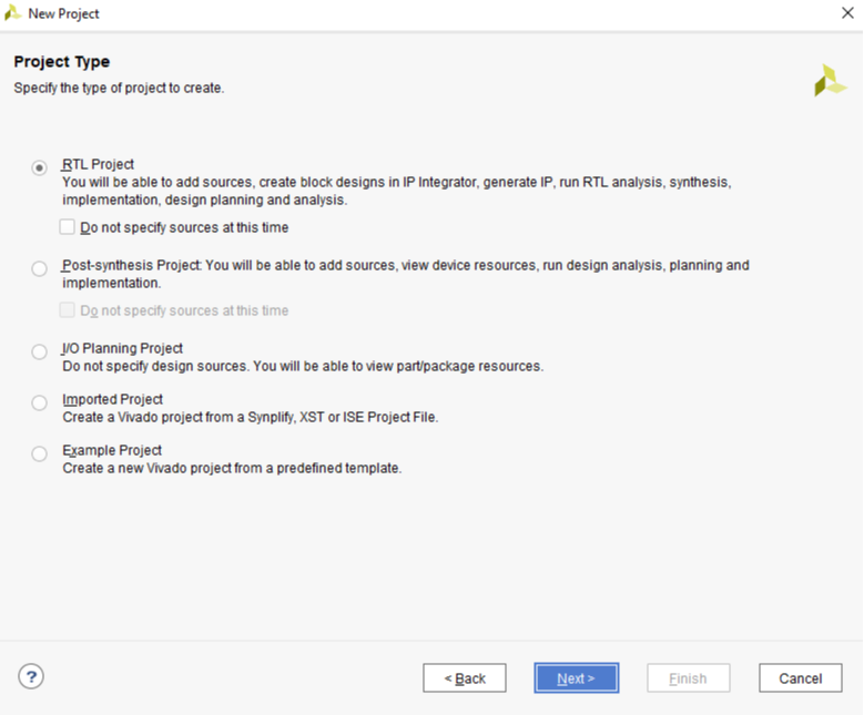
Select Project Type
The “project type” configures certain design tools and the IDE appearance based on the type of project you are intending to create. Most of the time, and for all Real Digital courses, you will choose “RTL Project” to configure the tools for the creation of a new design. (RTL stands for Register Transfer Language, which is a term sometimes used to mean a hardware design language like Verilog).
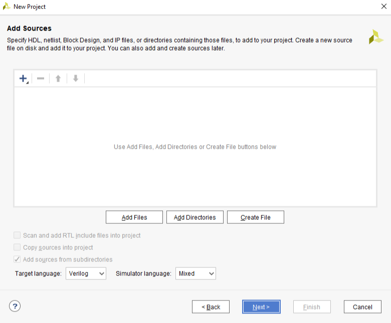
Add Existing Sources
In a typical new or early-stage design, you won’t add any existing sources because you haven’t created them yet. But as you complete more designs and build up a library of previously completed and known good designs, you may elect to add sources and them use them in a new design.
For now, there are no existing sources to add, so just click Next.
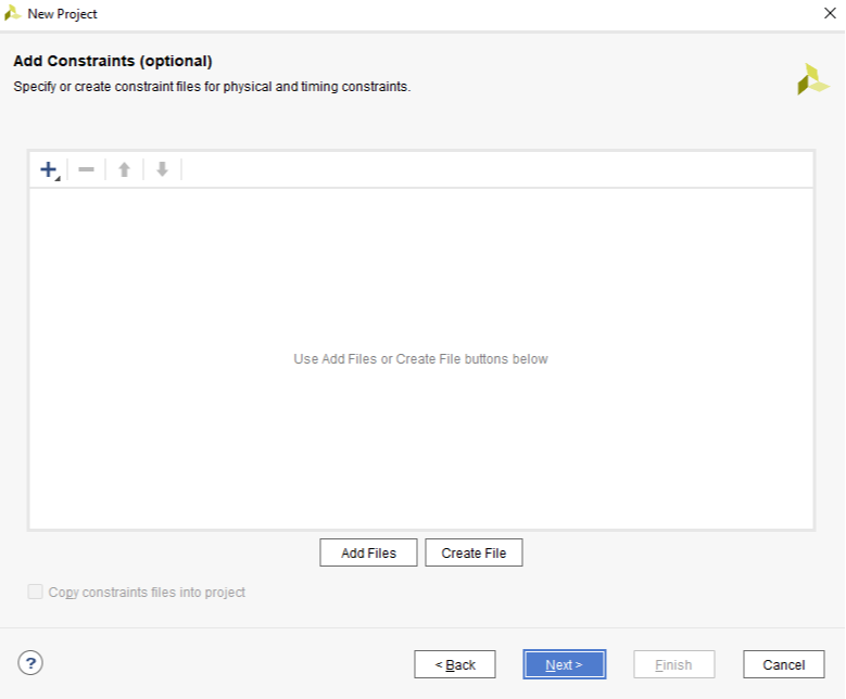
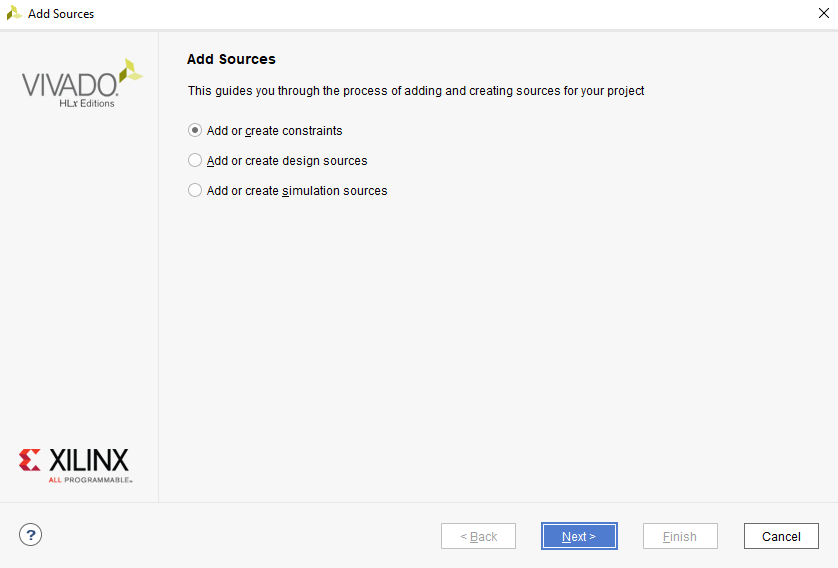
Add Constraints
Constraint files provide information about the physical implementation of the design. They are created by the user, and used by the synthesizer. Constraints are parameters that specify certain details about the design. As examples, some constraints identify which physical pins on the chip are to be connected to which named circuit nodes in your design; some constraints setup various physical attributes of the chip, like I/O pin drive strength (high or low current); and some constraints identify physical locations of certain circuit components.
The Xilinx Design Constraints (.xdc filetpye) is the file format used for describing design constraints, and you need to create an .xdc file in order to synthesize your designs for a Real Digital board. Later in this tutorial, you will create a constraints file to identify which named circuit nodes must be connected to which physical pins. But for now, you have no existing constraints file to add, so you can simply click next.
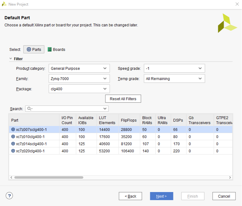
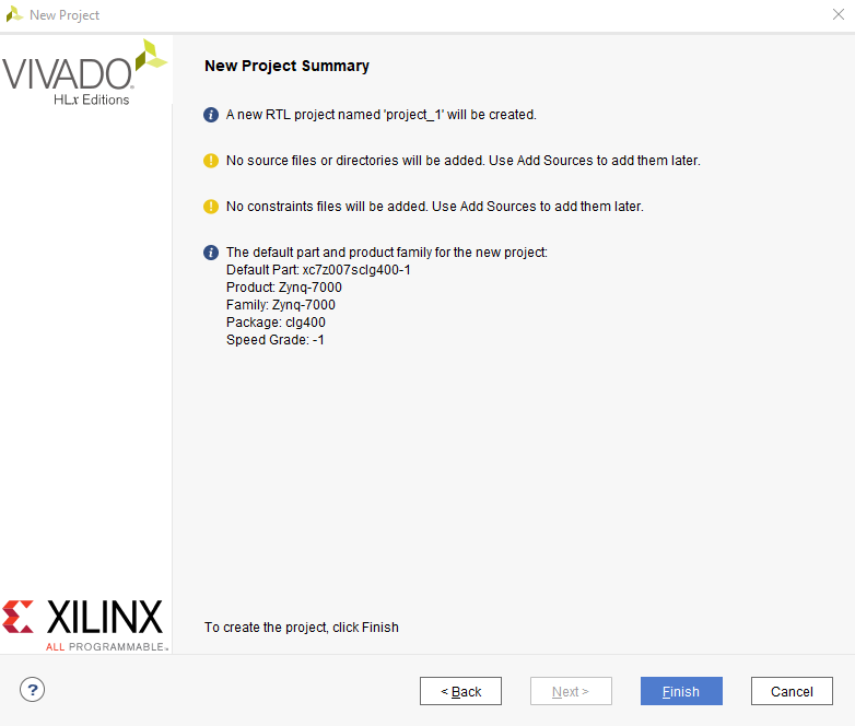
Select Parts
Xilinx produces many different parts, and the synthesizer needs to know exactly what part you are using so it can produce the correct programming file. To specify the correct part, you need to know the device family and package, and less critically, the speed and temperature grades (the speed and temperature grades only affect special-purpose simulation results, and they have no effect on the synthesizer’s ability to produce accurate circuits). You must choose the appropriate part for the device installed on your board.
For example, the Blackboard uses a zynq device with the following attributes:
| Part Number | xc7z007sclg400-1 |
|---|---|
| Family | Zynq-7000 |
| Package | clg400 |
| Speed Grade | -1 |
| Temperature Grade | C |
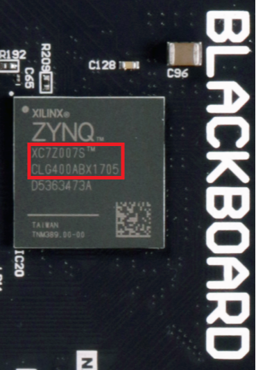
How to find your Zynq 7000 SoC Parts
You can find the details about your xilinx part from the markings on the IC, in the reference manual for your board, on the page where you purchased the board, or in the board’s schematic.
From Identeifcation Marking on IC
Usually, you can find the part number directly from the marking on the surface of the logic device. In the picture below, you can see the part number for a Zynq-7000 device found on a Blackboard.
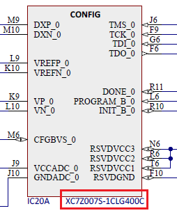
From Board Schematic
You can also find the part number from your board’s schematic. The figure below shows the Blackboard’s Zynq-7000 dvice identified in its schematic.
Check Project Configuration Summary
On the last page of the Create Project Wizard a summary of the project configuration is shown. Verify all the information in the summary is correct, and in particular make sure the correct FPGA part is selected. If anything is incorrect, click back and fix it; otheriwse, click Finish to finish creating an empty project.
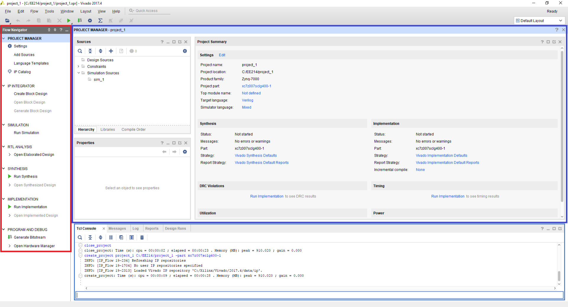
Vivado Project Window
After you have finished with the Create Project Wizard, the main IDE window will be displayed. This is the main “working” window where you enter and simulate your Verilog code, launch the synthesizer, and program your board. The left-most pane is the flow navigator that shows all the current files in the project, and the processes you can run on those files. To the right of the flow navigator is the project manager window where you enter source code, view simulation data, and interact with your design. The console window across the bottom shows a running status log. Over the next few projects, you will interact with all of the panels.
Step 2: Edit The Project - Create source files
All projects require at least two types of source files – an HDL file (Verilog or VHDL) to describe the circuit, and a constraints file to provide the synthesizer with the information it needs to map your circuit into the target chip.
This tutorial presents the steps required to implement a Verilog circuit on your Real Digital board: first, a Verilog source file is created to define the circuits behavior (again, for this tutorial, you can simply copy or download the completed file rather than typing it); second, a constraints files is created to define how the Verilog circuit is mapped into the Xiling logic device (again, copied or downloaded for this tutorial); third, the Verilog source file and constraints file are synthesized into a “.bit” file that can be programmed onto your board; and fourth, the device is configured with the circuit.
After the Verilog source file is created, it can be directly simulated. Simulation (discussed in more detail later) lets you work with a computer model of a circuit, so you can check its behavior before taking the time to implement it in a physical device. The simulator lets you drive all the circuit inputs with varying patterns over time, and to check that the outputs behave as expected under all conditions.
After the constraint file is created, the design can be synthesized. The synthesis process translates Verilog source code into logical operations, and it uses the constraints file to map the logical operations into a given chip. In particular (for our needs here), the constraints file defines which Verilog circuit nodes are attached to which pins on the Xilinx chip package, and therefore, which circuit nodes are attached to which physical devices on your board. The synthesis process creates a “.bit” file that can be directly programmed into the Xilinx chip.
In this first tutorial, the Verilog and constraint source files are provided for you. Instead of creating them yourself as would normally be the case, you can simply copy them into empty source files, or download them and include them in your project directly. In later designs, you will create these files yourself.
Design Sources
There are many ways to define a logic circuit, and many types of source files including VHDL, Verilog, EDIF and NGC netlists, DCP checkpoint files, TCL scripts, System C files, and many others. We will use the Verilog language in this course, and introduce it gradually over the first several projects. For now, you can get familiar with some of the basic concepts by reading the following.
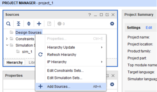
To create a Verilog source file for your project, right-click on “Design Sources” in the Sources panel, and select Add Sources. The Add Sources dialog box will appear as shown – select “Add or create design sources” and click next.

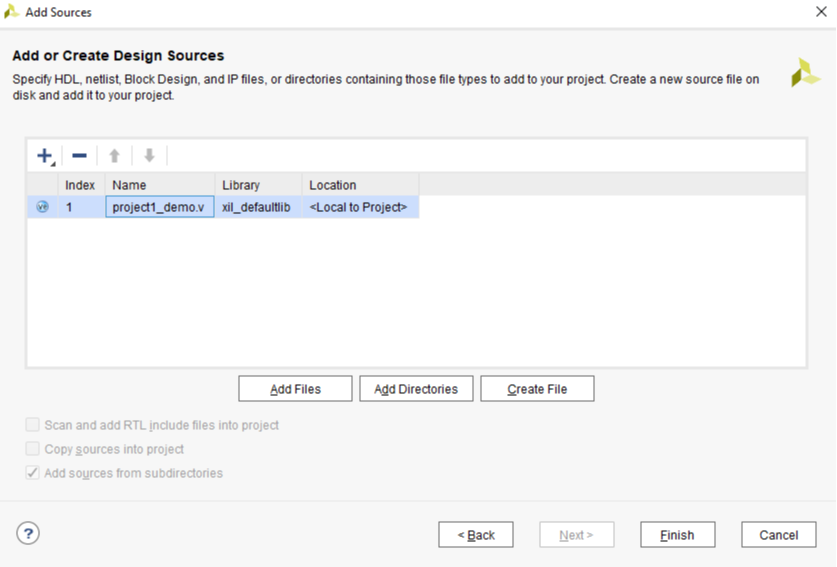
In the Add or Create Design Sources dialog, click on Create File, enter project1_demo as filename, and click OK. The newly created file will appear in the list as shown. Click Finish to move to the next step.
Skip the Define Module dialog by clicking OK to continue.
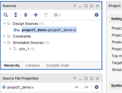
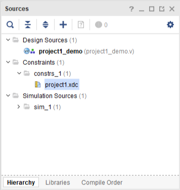
You will now see
project1_demolisted underneath Design Sources folder in the Sources panel. Double clickproject1_demoto open the file, and replace the contents (copy and paste) with the code below.
Alternative: Download and Add Source
Instead of creating a source file by using copy and paste as described above, you can alternatively download the project1_demo.v file and add it to your project using the Add Sources button in Add Sources dialog.
`timescale 1ns / 1ps

    module project1_demo(
        input clk,
        output [15:0] led,
        output [7:0] seg,
        output [3:0] an
    );

    reg [23:0] counter = 24'd0;
    reg divclk = 1'b0;
    reg [3:0] round_counter = 4'd0;
    reg [15:0] led_reg;
    reg [7:0] seg_reg;

    /* Clock Divider: 100MHz -> 10Hz (100ms) */
    always @(posedge clk)
    begin
        if (counter == 24'd4999999) begin
            divclk <= ~divclk;
            counter <= 24'd0;
        end
        else begin
            divclk <= divclk;
            counter <= counter + 1'd1;
        end
    end

    always @(posedge divclk)
    begin
        round_counter <= round_counter + 1'd1;
    end

    always @(posedge divclk)
    begin
        if (round_counter == 4'd0) begin
            led_reg <= 16'hFFFE;
            seg_reg <= 8'hFE;
        end
        else begin
            seg_reg <= {seg_reg[6:0], seg_reg[7]};
            led_reg <= {led_reg[14:0], led_reg[15]};
        end
    end

    assign led = led_reg;
    assign an = 4'h0;
    assign seg = seg_reg;

    endmodule
Design Constraints
Design sources, like Verilog HDL files, only describe circuit behavior. You must also provide a constraints file to map your design into the physical chip and board you are working with.
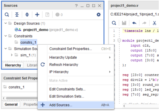
To create a constraint file, expand the Constraints heading in the Sources panel, right-click on constrs_1, and select Add Sources.
An Add Sources dialog will appear as shown. Select Add or Create Constraints and click Next to cause the “Add or Create Constraints” dialog box to appear.
Click on Create File, enter project1 for the filename and click OK. The newly created file will appear in the list as shown. Click Finish to move to the next step.
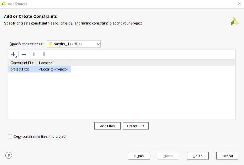
You will now see project1.xdc listed underneath Constraints/constrs_1 folder in the Sources panel. Double click project1.xdc to open the file, and replace the contents with the code below.
Alternative: Download and Add Constraints
Instead of creating an empty constraint file and using copy-and-paste to replace the contents as described above, you can also download the project1.xdc file and add it to your project using the Add Files button in Add Sources dialog.
##Clock
#IO_L13P_T2_MRCC_35 Schematic name=SYSCLK
set_property -dict { PACKAGE_PIN H16   IOSTANDARD LVCMOS33 } [get_ports { clk }];
create_clock -add -name sys_clk_pin -period 10.00 -waveform {0 4} [get_ports { clk }];

##LEDS
#IO_L14P_T2_SRCC_34 Schematic name=LD0
set_property -dict { PACKAGE_PIN N20   IOSTANDARD LVCMOS33 } [get_ports { led[0] }];
#IO_L14N_T2_SRCC_34 Schematic name=LD1
set_property -dict { PACKAGE_PIN P20   IOSTANDARD LVCMOS33 } [get_ports { led[1] }];
#IO_0_34 Schematic name=LD2
set_property -dict { PACKAGE_PIN R19   IOSTANDARD LVCMOS33 } [get_ports { led[2] }];
#IO_L15P_T2_DQS_34 Schematic name=LD3
set_property -dict { PACKAGE_PIN T20   IOSTANDARD LVCMOS33 } [get_ports { led[3] }];

##RGB_LEDS
#IO_L3P_T0_DWS_PUDC_B_34 Schematic name=LD4_R
set_property -dict { PACKAGE_PIN U13   IOSTANDARD LVCMOS33 } [get_ports { led[4] }];
#IO_25_34 Schematic name=LD4_G
set_property -dict { PACKAGE_PIN T19   IOSTANDARD LVCMOS33 } [get_ports { led[5] }];
#IO_L16N_T2_34 Schematic name=LD4_B
set_property -dict { PACKAGE_PIN W20   IOSTANDARD LVCMOS33 } [get_ports { led[6] }];

#IO_L17N_T2_34  Schematic name=LD5_R
set_property -dict { PACKAGE_PIN Y19   IOSTANDARD LVCMOS33 } [get_ports { led[7] }];
#IO_L16P_T2_34 Schematic name=LD5_G
set_property -dict { PACKAGE_PIN V20   IOSTANDARD LVCMOS33 } [get_ports { led[8] }];
#IO_L22N_T3_34 Schematic name=LD5_B
set_property -dict { PACKAGE_PIN W19   IOSTANDARD LVCMOS33 } [get_ports { led[9] }];

#IO_L22P_T3_34  Schematic name=LD6_R
set_property -dict { PACKAGE_PIN W18   IOSTANDARD LVCMOS33 } [get_ports { led[10] }];
#IO_L18N_T2_34 Schematic name=LD6_G
set_property -dict { PACKAGE_PIN W16   IOSTANDARD LVCMOS33 } [get_ports { led[11] }];
#IO_L17P_T2_34 Schematic name=LD6_B
set_property -dict { PACKAGE_PIN Y18   IOSTANDARD LVCMOS33 } [get_ports { led[12] }];

#IO_L8N_T1_34 Schematic name=LD7_R
set_property -dict { PACKAGE_PIN Y14   IOSTANDARD LVCMOS33 } [get_ports { led[13] }];
#IO_L7P_T1_34 Schematic name=LD7_G
set_property -dict { PACKAGE_PIN Y16   IOSTANDARD LVCMOS33 } [get_ports { led[14] }];
#IO_L7N_T1_34 Schematic name=LD7_B
set_property -dict { PACKAGE_PIN Y17   IOSTANDARD LVCMOS33 } [get_ports { led[15] }];

##SevenSegmentDisplay
##anodes
#IO_L10P_T1_AD11P_35 Schematic name=SSEG_AN0
set_property -dict { PACKAGE_PIN K19   IOSTANDARD LVCMOS33 } [get_ports { an[0] }];
#IO_L13N_T2_MRCC_35 Schematic name=SSEG_AN1
set_property -dict { PACKAGE_PIN H17   IOSTANDARD LVCMOS33 } [get_ports { an[1] }];
#IO_L8N_T1_AD10N_35 Schematic name=SSEG_AN2
set_property -dict { PACKAGE_PIN M18   IOSTANDARD LVCMOS33 } [get_ports { an[2] }];
#IO_L11P_T1_SRCC_35 Schematic name=SSEG_AN3
set_property -dict { PACKAGE_PIN L16   IOSTANDARD LVCMOS33 } [get_ports { an[3] }];

##cathodes
#IO_L20P_T3_AD6P_35 Schematic name=SSEG_CA
set_property -dict { PACKAGE_PIN K14   IOSTANDARD LVCMOS33 } [get_ports { seg[0] }];
#IO_L19P_T3_35 Schematic name=SSEG_CB
set_property -dict { PACKAGE_PIN H15   IOSTANDARD LVCMOS33 } [get_ports { seg[1] }];
#IO_L14P_T2_AD4P_SRCC_35 Schematic name=SSEG_CC
set_property -dict { PACKAGE_PIN J18   IOSTANDARD LVCMOS33 } [get_ports { seg[2] }];
#IO_25_35 Schematic name=SSEG_CD
set_property -dict { PACKAGE_PIN J15   IOSTANDARD LVCMOS33 } [get_ports { seg[3] }];
#IO_L8P_T1_AD10P_35 Schematic name=SSEG_CE
set_property -dict { PACKAGE_PIN M17   IOSTANDARD LVCMOS33 } [get_ports { seg[4] }];
#IO_L24N_T3_AD15N_35 Schematic name=SSEG_CF
set_property -dict { PACKAGE_PIN J16   IOSTANDARD LVCMOS33 } [get_ports { seg[5] }];
#IO_L8P_T1_AD10P_35 Schematic name=SSEG_CG
set_property -dict { PACKAGE_PIN H18   IOSTANDARD LVCMOS33 } [get_ports { seg[6] }];
#IO_L12N_T1_MRCC_35 Schematic name=SSEG_DP
set_property -dict { PACKAGE_PIN K18   IOSTANDARD LVCMOS33 } [get_ports { seg[7] }];
Step 3: Synthesize, Implement, and Generate Bitstream
Synthesis
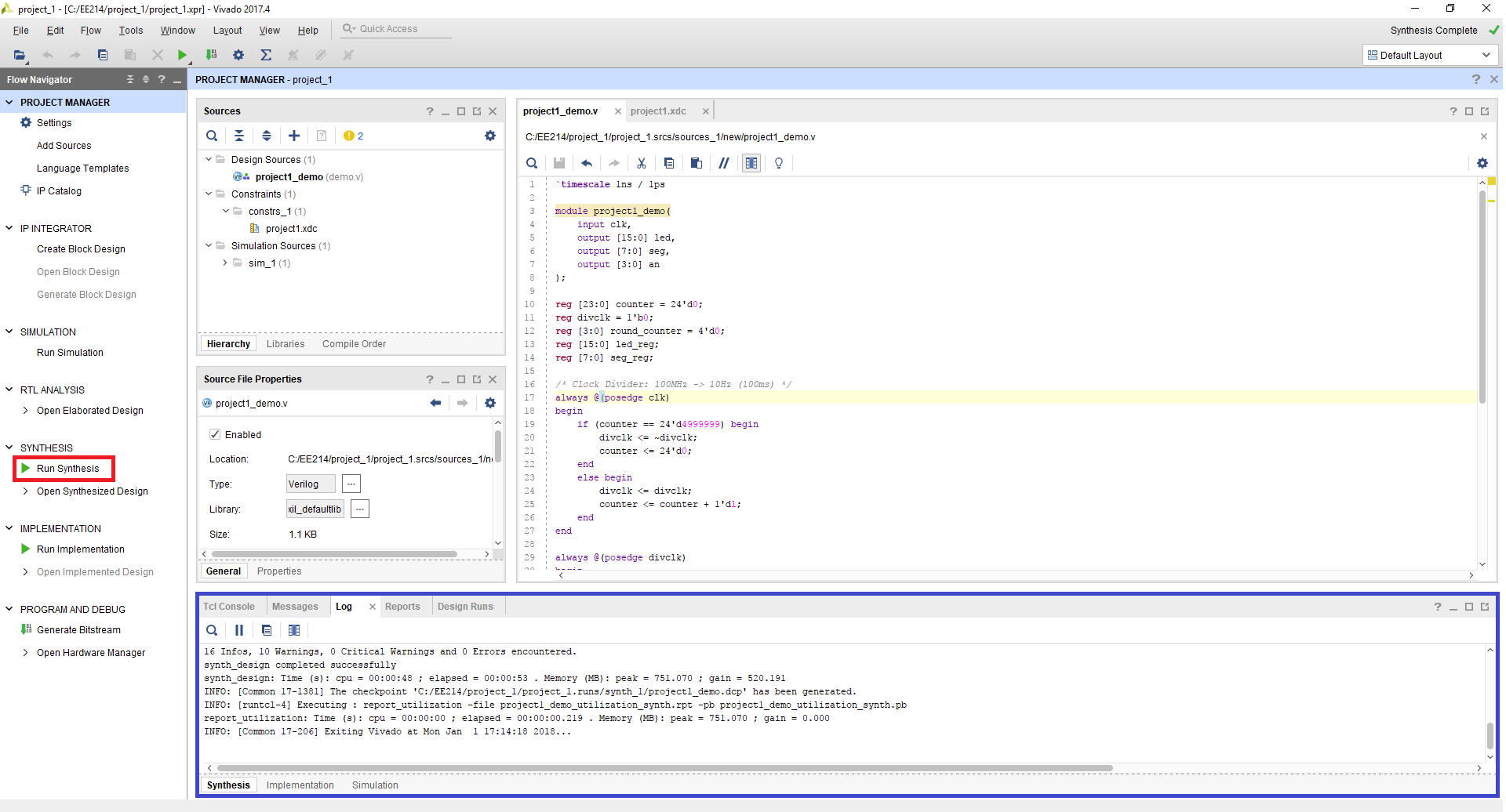
After your Verilog and constraint files are complete, you can Synthesize the design project. In the synthesis process, Verilog code is translated into a “netlist” that defines all the required circuit components needed by the design (these components are the programmable parts of the targeted logic device - more on that later). You can start the Synthesize process by clicking on Run Synthesis button in the Flow Navigator panel as shown.
When synthesis is running, you can select the log panel located at the bottom of Project Manager to see a log of the currently running processes. Any errors that occur during the synthesis process will be described in the log.
Implementation
After the design is synthesized, you must run the Implementation process. The implementation process maps the synthesized design onto the Xilinx chip targeted by the design. Click the Run Implementation button in the Flow Navigator panel as shown.
When the implementation process is running, the log panel at the bottom of Project Manager will show details about any errors that occurr.
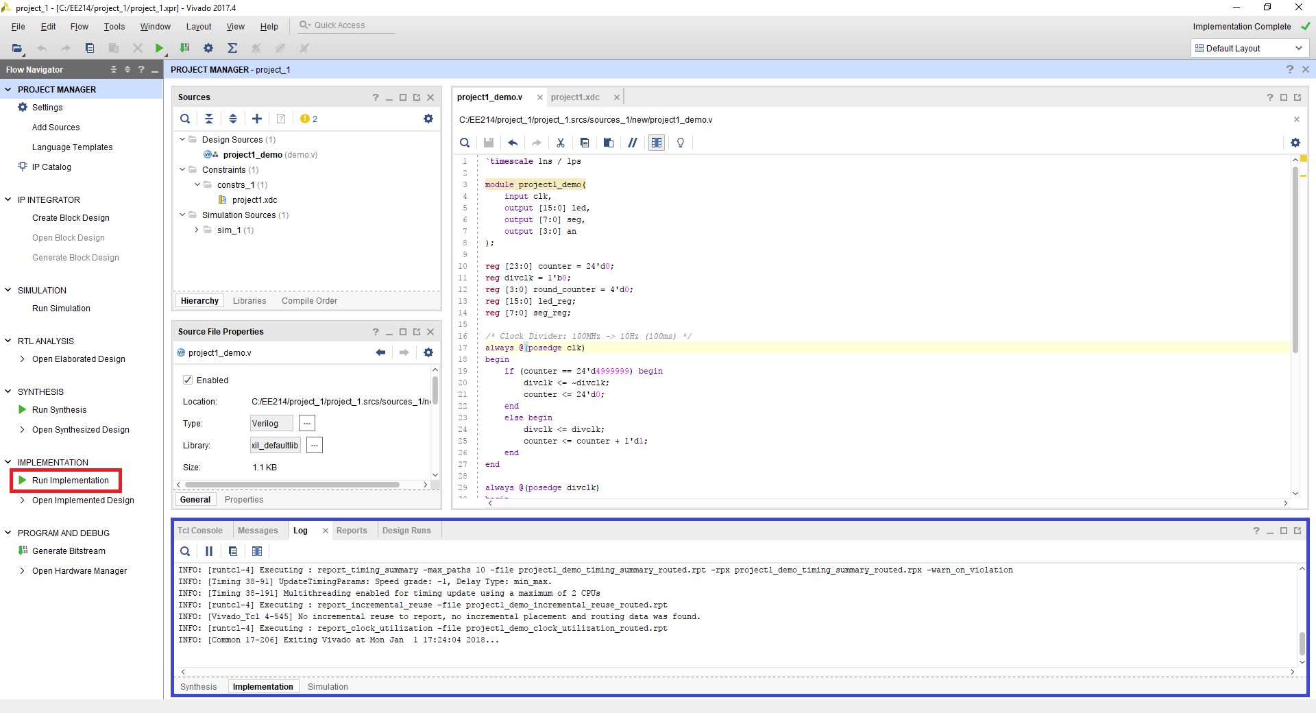
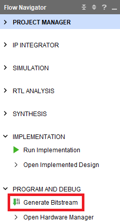
Generate Bitstream
After the design is successfully implemented, you can create a .bit file by clicking on the Generate Bitstream process located in the Flow Navigator panel as shown. The process translates the implemented design into a bitstream which can be directly programmed into your board’s device.
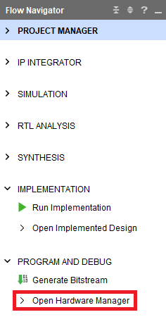
Step 4: Download Bitstream
Open Hardware Manager
After the bitstream is successfully generated, you can program your board using the Hardware Manager. Click Open Hardware Manager located at the bottom of Flow Navigator panel, as highlighted in red in the Figure.
Connecting Your Board via USB
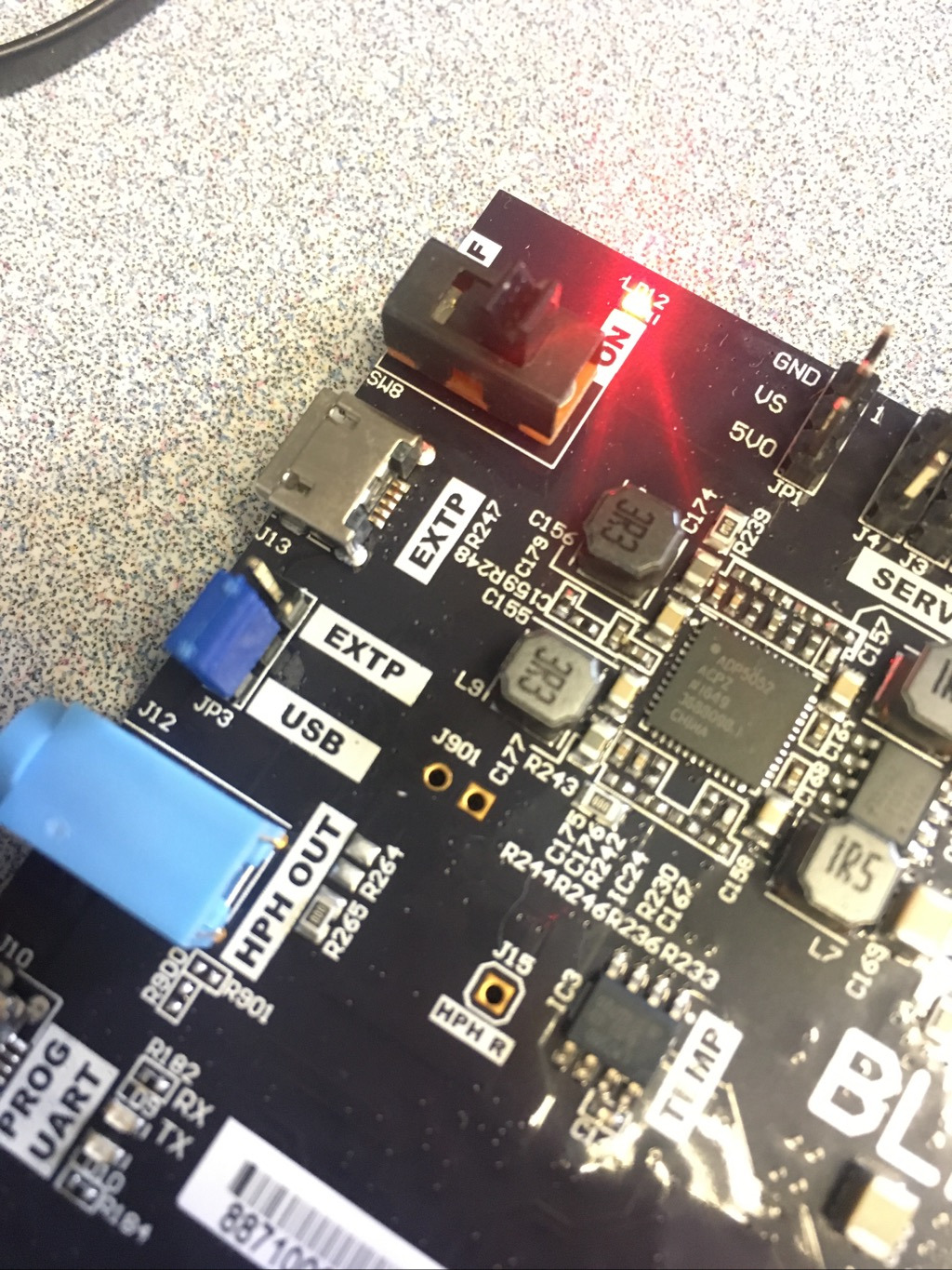
Connect your Blackboard to your Computer with a micro-USB cable. Make sure you connect the micro-USB cable to the port labeled “PROG UART”. Turn on your board by moving the switch in the top-left corner to the on position. You’ll see a red LED light up by the switch when it powers on. If your board doesn’t power on, check that the blue jumper by the port labeled “EXTP” is set to “USB”. The figure shows a powered on Blackboard, with the correct jumper setting.
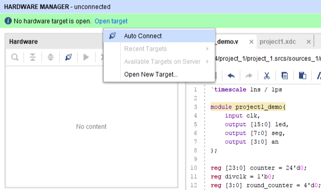
Connecting your Board to Vivado
Click on Open target link underneath Hardware Manager. Select Auto Connect to automatically identify your board.
If you’re having trouble connecting in Linux you may need to install cable drivers. Follow the tutorial: TUTORIAL: Installing Linux Cable Drivers
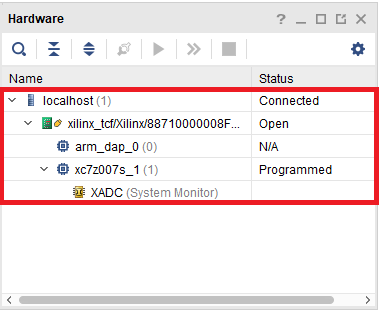
Verify that Your Board is Identified
If Vivado successfully detects your board, the Hardware panel (located at the top left corner of Hardware Manager) will show the board’s logic device part number (For the Blackboard this will be xc7z007s).
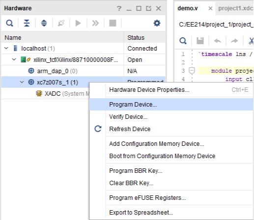
Download Bitstream
Select the device you want to program, right click and select Program Device. A Program Device pop-up dialog window will appear, with the generated bit file selected in the text box. Click on Program to download the bitstream to your board.