A Second Tutorial: Controlling LEDs with Switches
Basic Verilog to define a simple circuit and connect it to Blackboard I/O devices

Introduction
This tutorial demonstrates how to describe a basic digital circuit using Verilog, and in particular, how to connect circuit inputs and outputs to physical devices on a Real Digital board. In this tutorial, slide switch inputs are connected through the your board’s Xilinx device to LED outputs, without any logic in between. This simple exercise is intended to demonstrate how input and output devices are connected to your circuits – in the next exercise, you will add logic circuits between the inputs and outputs.
Basic digital circuits receive information from the “outside world” in the form of digital signals. Recall digital signals are voltage signals that are constrained to be at the circuits “high” voltage (typically 3.3V, also called a ‘1’), or the circuits “low” voltage (or ground, also called a ‘0’). Although signals are wires that transport voltage, we tend to think of digital signals as transporting information (a ‘0’ or a’1’).
A basic digital circuit combines and manipulates information transported by input signals (‘0’ or ‘1’) using various logical constructs like AND’ing or OR’ing, and produces one or more output signals that return information to the “outside world”. Within the digital circuit, there are typically several signals that transport information between devices inside the circuit, and that never see the outside world; and there are several signals called “ports” that communicate with the outside world. In the example circuit shown below, the input port signals A, B, and C are connected to pushbuttons, and the output ports are connected to LEDs.

There are many devices and sources that can drive input port signals, including pushbuttons, slide switches, keyboards, touch panels, other electronic devices. Likewise, there are many devices that might receive output port signals, like LEDs, speakers, actuators, other electronic devices, etc. Your Real Digital board contains several input and output devices that can produce and consume I/O port signals. In this tutorial, a slide switch is used as an input device, and an LED is used as an output.
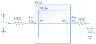
A Simple Circuit
We will build a simple circuit called led_sw that passes a signal through a Xilinx logic device, from an input slide switch to an output LED, without using any other components. The input port is called “sw”, and the output port is called “led”. Only a single assign statement is needed in the Verilog code to connect the “sw” input to the “led” output, and this is shown below. But recall the Verilog description is only part of the solution - we must also connect the “logical” circuit names in our design (i.e., sw and led) to the physical pins on the Xilinx device – in this case, to the pins connected to the switch and LED we wish to use.
To connect logical signal names in a Verilog source file to physical pins on the ZYNQ device, Xilinx requires “pin mapping” statements in an “.xdc file” (xdc stands for “Xilinx Design Constraints”). A part of the Blackboard schematic and a view of the ZYNQ chip are shown below. The yellow boxes in the schematic show LD0 is connected to ZYNQ pin N20, and SW0 is connected to pin R17. By examining the bottom view of the chip and it’s pin definition graphic (taken from Xilinx UG865 at www.xilinx.com), you can find those two pins on the ZYNQ chip package. Small copper wires in the PCB electrically connect those pins to SW0 and LD0. Since SW0 is connected by a copper wire to ZYNQ pin R17, any Verilog signal name tied to pin R17 will be driven to a ‘0’ or ‘1’ by SW0. Likewise, since ZYNQ pin N20 is connected by a copper wire to LD0, driving a ‘1’ or ‘0’ on a Verilog output port signal tied to LD0 will turn the LED on or off. Entries in the .xdc file make the associations between your Verilog signal names and the physical pins. A little later in this tutorial, we’ll show you how to create the required entries in the .xdc file.

Step 1: Create a new project
Create an empty project named requirement_2 (or something similar) following the procedure introduced in the previous tutorial.
Step 2: Design the circuit in Verilog HDL
Create and add a Verilog source file named led_sw.v to your project. If you can’t remember how, refer to the previous tutorial.
Begin the Verilog file by typing the module statement. In any Verilog source file, the first statement is the “module” statement that provides a name for the module and declares the input and output port signals. The format shown below is generic. The keyword “module” is followed by an alpha-numeric text string that provides the module’s name, and a list of port signals and their direction (in parenthesis). The keywords “input” and “output” are followed by the names of input and output signals, in any order. Any number of input and output signals can be declared. In this example, you can name the module “led_sw”, and declare one output signal named “led” and one input signal named “sw”.
module led_sw(
    output led,
    input sw
);
The input and output signals “sw” and “led” are recognized as single wires. You can also declare groups of related signals that are organized as “buses”. The statements below declare 8 inputs grouped together in a bus named “sw”, and 8 output signals grouped together as a bus named “led”. This defines eight input signals named sw(7), sw(6), etc., and eight output signals named led(7), led(6), etc. using simple, single-line declarations. Note you can access individual signals on a bus by using the root name and the signal index in parenthesis (so, for example, sw(4) is the name of the 5th least significant signal on the sw bus).
input [7:0] sw
output [7:0] led;
Following the module statement, you can write any number of “assign” statements to define combinational logic circuits. The keyword “assign” is used in Verilog any time you want to assign a value to a wire. Simple assignments, like “assign led = sw”, can be used to map one signal onto another. More complex assignments can assign the result of logic operations to a wire, like “assign X = A | B & C” – these types of assignment will be used in the next exercise.
assign led = sw;
Assignment statements can work on individual signals or buses. For example, if “led” and “sw” are both declared as wires, then the statement “assign led = sw” will map a single signal. But if “led” and “sw” are declared as busses, then the same assign statement will assign multiple signals, from right-most (least significant) input bus signal to right-most (least significant) output bus signal, and then the next-least-significant input to the next-least-significant output, etc., until one of the busses has no more signals.
When all required assign statements have been added to the Verilog file, the module description is ended with the “endmodule” key word.
Verilog Source File
When you have completed the previous steps, your Verilog source file should look like this:
`timescale 1ns/1ps
module led_sw(
    output led,
    input sw
);

assign led = sw;

endmodule
Step 3: Add Constraints (XDC)
Recall that before a circuit can be implemented on your Xilinx device, all the external pin connections must be defined in a constraints file. Create and add an empty constraints file named project2.xdc to your project. If you can’t remember how, refer to the previous tutorial. Add two entries into your xdc constraints file – one for the input switch, and one for the output LED as shown below. In a later module, the syntax and meaning of the .xdc entries will be explained more fully.
The general form to make a pin mapping is shown below; The device pin to map to follows PACKAGE_PIN and the logical net defined in your verilog file is placed between the braces after get_ports. The example shows the logical net sw being mapped to the pin R17 (on the Blackboard this is SW0).
#Map Pin R17 to the net wire sw
set_property -dict { PACKAGE_PIN R17   IOSTANDARD LVCMOS33 } [get_ports { sw }];
If you are mapping signals defined as a bus (e.g. sw[7:0] ), each entry needs a mapping in the XDC file, as a bus is just a logical grouping of single nets. To map an index of a bus type the bus name followed by brackets containing the index desired; For the fourth wire in sw[7:0], you can use sw[3].
Note: Typing in all the individual pin constraints can be time consuming. Instead, you can download and add the corresponding “master” .xdc file for your board to your project (or alternatively, you can create your own .xdc file and cut-and-paste the attached file contents into it). Each Real Digital board’s master .xdc file defines all of the pin connections to external devices (switches, LEDs, etc). Any “extra” signals defined in the master .xdc file should be comented out by placing a pound sybol at the start of the line. In the .xdc file linked on the right, several of the signals we will not use in this class have been commented-out.
Step 4: Generate a .bit file, and test your design
Run synthesis, implementation, and generate bitstream as shown in the previous tutorial. Download your circuit to your board using the Hardware Manager.