Project 7 Latches and Flip-Flops
The basic memory elements used in sequential circuits

Introduction
This project introduces the concept of electronic memory in digital circuits. Digital circuits need memory in order to create ordered sequences of events, like playing one note after another to reproduce a digitized song, or to track and respond to sequences of events, like ensuring a particular sequence of button presses is used to open a digital combination lock.
Most digital circuits use electronic memory. Electronic memory circuits store the state of an input signal at some particular time, and their memorized outputs (or data) can be used at a later time. Digital circuits that use electronic memory are called sequential circuits, because they can use memorized data to create or sense ordered sequences of events. In contrast, combinational circuits do not use memory, and so they can only change their outputs to reflect the current state of their inputs. Creating sequences is fundamental to all of computing, and many 100’s of billions of computing circuits are in use today.
This project presents two of the most common memory devices used in digital circuit design - the D-latch and D-flip-flop. Both devices memorize a single input when triggered by a timing signal, and both have a single output that always shows the state of the memorized signal. They differ in how they respond to the timing signal – the D-latch allows an input signal to flow into and through it whenever the timing signal is asserted, but the D-flip-flop only “samples” (or reads) an input at the rising edge of the timing signal.
Before you begin, you should:
- Have a good amount of experience using Vivado and the Blackboard;
- Beable to write and execute a Verilog testbench;
- Know how to model and simulate circuit delays.
After you’re done, you should:
- Understand the operation of an S-R latch;
- Understand the cause of metastability;
- Understand the operation of latches and flip-flops;
- Be able to describe memory circuits in behavioral Verilog.
Background
Digital systems use memory circuits to “memorize” the state of certain signals (a ‘1’ or a ‘0’), and then they use those memorized signals to help determine future signal transitions. Simple memory circuits can be constructed using NAND or NOR gates. These circuits memorize a signal value by driving a feedback loop into one of two stable states (storing a ‘0’ or storing a ‘1’), and the stored value continuously drives an output signal. Because there are only two intended stable states, binary memory devices are termed “bistable” devices. The memory circuit’s feedback loop will remain in one of the two bistable states until new inputs arrive and force a change.
The simple circuit that creates the feedback loop necessary to create memory is most typically used as a component in a higher-level memory device. The two most common higher level circuits/devices are called a D-Latch and a D-flip-flop. Both devices have one data input, one timing control input, and one output. In operation, the input signal is memorized when the timing signal is asserted. Note the memory circuit output can only change in response to the timing signal – the data signal can change all it wants, but it can’t effect the memory circuit until the timing signal is asserted.

All memory circuits drive their outputs to match their inputs when the timing signal is asserted, and they ignore input signal changes when the timing signal is inactive. Besides the D-latch and D-flip-flop used in digital circuit design, there are several other types of memory circuits that are in commonly use as well.
Computer memory systems that store programs/applications and their data use very small and inexpensive “dynamic” memory circuits. These dynamic memory cells use stores of charged particles held on tiny capacitors to represent signal values. It is difficult to construct high quality capacitors on a CMOS chip, and so these tiny capacitors leak. Whatever charge was stored on them (representing a ‘1’ or a ‘0’) must be “refreshed” (or rewritten) every 100ms or so because of the leaks. To deal with these leaks, dynamic memory circuits use special refresh controller circuits that continuously revisit and recharge every storage cell. Dynamic memories also require precision, high-speed amplifiers that can sense the small amount of charge stored on the capacitors. For memory arrays exceeding 1 billion bits (not large by today’s standards), these overhead requirements don’t add much to the cost of 1 bit of memory. But for the small number of bits used in a typical digital circuit design, the overhead is too much.
Smaller, faster computer memory arrays can use “static” memory cells that store input signal values in self-stabilizing feedback loops. These memory cells are much larger than the single, tiny capacitors used in dynamic memory cells. They are also faster, and they don’t leak (and so they don’t need to be refreshed). But they do need special driver circuits to change the memorized signal stored in the feedback loop, and this (together with the larger memory cell size) limits the size of static memory arrays to millions of bits (not billions). Static memory cells are often used as cache memories, or for small, high-speed on-chip memory arrays. But, as with dynamic memory, the overhead required to manage static memory arrays makes them less attractive for use in simpler, smaller digital circuits (although they are better suited than dynamic memory cells).
Digital circuits typically only need dozens, or perhaps hundreds of bits of storage to memorize their operating “state” (the operating state of a digital circuit will be define more precisely a bit later). When so few bits of storage are required, there is no need to use the smallest possible memory cell and suffer with the overhead requirements. Rather, memory cells with lower overhead and that are easier to use are appropriate. These memory cells are the D-Latch and D-flip-flop mentioned earlier, and they are the subject this design project.
This project will start by examining the basic feedback memory circuits called “basic cells” that are used as components of latches and flip-flops. Then, the latches and flip-flops will be presented and used in various circuits. Finally, components built from groups of flip-flops called “registers” are examined. Registers are used to simultaneously memorize all the bits of a bus, so that binary numbers can stored as integral units (see the Registers topic document for more information).
Requirements
1. Implement and simulate a NAND basic cell
First, complete the tutorial: TUTORIAL: SR-LATCH and D-Latch
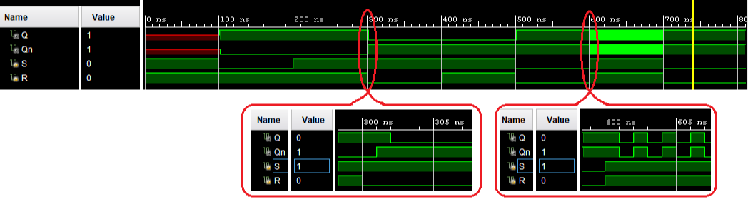
Examine the output of your simulation (and figure 1 below shows a similar simulation). In the simulation below, the reset signal is asserted at 300ns (the zoomed-in graph on the left shows a more detailed view). Note that it takes 2 ns for the reset signal R to propagate through the NAND cell (this is due to the 1ns gate delays you added into your simulation). Then at 600 ns, both set (S) and reset toggle from 0 to 1 at exactly the same time. When S and R are deasserted exactly simultaneously, the basic cell tries to enter the hold condition from the ambiguous condition of being directed to both set and reset at the same time. This sets up an oscillation, based on the gate delays we chose. In an actual, physical circuit, this high-speed oscillation may drive the basic cell output from rail to rail at the same oscillation frequency, or due to pin loading, the output voltage may only change by a few hundered millivolts. In any case, this is an unstable condition that is commonly referred to as “meta-stability”.
2. Implement and simulate a NOR basic cell
Based on your NAND basic cell desgin, implement and simulate a NOR basic cell. Create a simulation input, and demonstrate the meta-stable behavior as before.
3. Design and simulate a D-Latch
Implement the D-Latch shown in the figure below. Simulate the latch and try to drive it into a metastable state. Refer to the background section for more information about D-latches.
Hint: A basic cell is driven into metastability by issuing a store operation before a set or reset operation is finished. Similarly, the D-Latch can be driven into stability by issuing a latching operation before the new data is updated to the D-Latch.

4. Parallel In Parallel Out (PIPO) Register
Define an 8-bit PIPO register in Verilog, with eight slide switches connected to the inputs. Connect each of the eight outputs to the “I1” input of a 2:1 mux, and connect the slide switches to the “I0” input of the mux. Connect the mux outputs to eight green LEDs, connect one pushbutton to the PIPO register’s clock input, and connect a second pushbutton to the mux select. Verify that you can use the first button to ‘memorize’ the switch positions, and use the second button to ‘recall’ them onto the LEDs.

Note: Clock signals and inputs are very noise sensitive, and the clock networks inside the FPGA carefully managed by the design tools. Under normal conditions, only certain signal sources are allowed to drive clock inputs, including dedicated clock input pins, the specialized “clock management tile” inside the FPGA, and signals arising directly from other flip-flops. For this requirement, you are asked to use a non-conforming input (from a pushbutton) as a clock signal to better illustrate basic operations. Vivado will only allow this if you include the line “set_property CLOCK_DEDICATED_ROUTE FALSE [get_nets btn[0]];” in the .xdc file.
Logic signals are often used to control when data is loaded in a register. Using a logic signal as a clock is generally considered poor design practice, for reasons that will be presented later. A far better solution is to drive the flip-flop’s clock from a proper clock source, and then use the logic signal as a “clock enable” signal. This protects the integrity of the clock network, while preserving the same functionality. Modify your code to connect the FPGA’s main clock to the clock input, and use btn[0] as an enable. The FPGA’s main clock signal is called clk in the .xdc file, so you must include clk as an input to your module. A complete .xdc file (that includes clock) for the Blackboard is provided - you can use this .xdc for all remaining projects in this course.

5. Parallel In Serial Out (PISO) Shift Register
Define and implement a 16-bit PISO register in Verilog, and use it to create a “circular” shift register (or more properly, a rotate circuit) where bit15 is shifted back into bit0. At each rising edge of the clock, all bits should shift left one position, and bit15 should shift into bit0.
The FPGA’s main clock is 100MHz, which is far too fast to use for visual verification of the shift register. In order to see data moving through the shift register, you must create a slower/divided clock. For now, you can use the code shown below, with cntr[25] serving as the shift register clock (counters and clock dividers are presented in the next project).
Use eight slide switches to independently load the upper and lower 8 bits of the register, and use two pushbuttons to select which eight register bits are enabled for loading. Connect the sixteen outputs to the 16 LEDs on the blackboard.

reg [25:0] cntr;

 always @ (posedge(clk))
    cntr <= cntr + 1;
Note: This video does not show the “circularity” of bit 16 shifting into bit 0. When you program this project, the inputted data bits will continuously shift through all 16 bits.
6. Serial In Parallel Out (SIPO) Shift Register
Define an 8-bit SIPO register in Verilog. Drive the clock input with the same slower clock signal (cntr[25]) that you used in the previous requirement, and use a pushbutton to drive the SDI signal. Connect the register outputs to eight green LEDs, and verify you can shift a data bit in to the register at every clock edge.
Challenge
1. Barrel Shifter
Define an 8-bit PIPO register and an 8-bit barrel shifter in Verilog. The barrel shifter must include a fill bit, and it must be able to shift or rotate left or right by up to 8 bits. Connect the eight slide switches to the register inputs, and also to the control inputs of the shifter. Use a pushbutton to clock data into the register. Connect the register outputs to the inputs of the barrel shifter, and connect the barrel shifter outputs to eight LEDs. Enter data into the register, and then use the slide switches to verify you can shift and rotate the data properly.